Quick Answer: Will AI Replace Semiconductor Engineers?
No, AI is not likely to replace semiconductor engineers as a whole. It will replace or compress some repetitive tasks in documentation, debug, regression triage, design-rule checking, routine optimisation and manufacturing analysis. The stronger impact is role redesign. Engineers who can supervise AI-assisted workflows, define constraints, validate evidence, manage verification intent and make cross-domain trade-off decisions will become more valuable. This matches current industry direction. Synopsys is already positioning AI as a way to improve chip design workflows, support documentation search, generate optimised code, assist debug and reduce manual effort, while Semiconductor Engineering continues to frame AI as a tool that changes design and verification work rather than removing the need for engineering judgement.
2026 Update: Why the AI Replacement Question Is Back
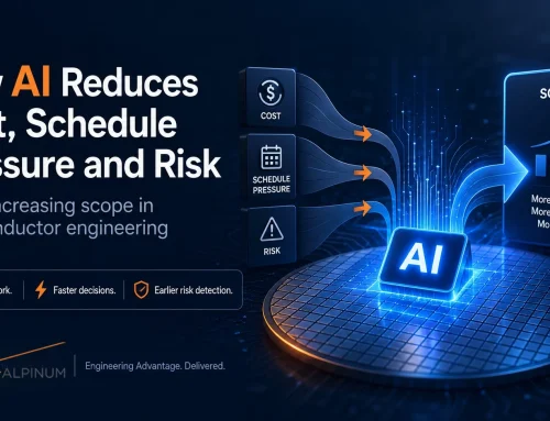
The question “will AI replace semiconductor engineers?” has become more urgent in 2026 because AI is no longer limited to generic productivity tools. It is now entering chip design, EDA workflows, verification support, manufacturing analytics and AI infrastructure planning.
Recent industry signals show why this matters. Synopsys has described generative and agentic AI as part of the next phase of chip design, with specialised AI agents supporting implementation, verification, analogue design and workflow movement. Siemens has also announced work with TSMC around AI-powered automation and advanced semiconductor design enablement, including automated fixing of design rule violations.
At the same time, demand for semiconductor capability is rising rather than shrinking. Reuters reported strong AI-driven demand across chip companies, including AMD, Arm and Infineon, while SEMI has warned that the industry still needs to add significant skilled engineering capacity by 2030. This means the more realistic outcome is not fewer engineers overall, but different engineering work, higher expectations and stronger demand for people who can combine domain knowledge with AI-assisted workflows.
For semiconductor leaders, the practical question is therefore not whether AI will replace engineers. The better question is where AI can safely reduce repetitive effort, where human review remains essential, and how engineering teams should redesign workflows before AI adoption creates new risk.
Will AI Replace Semiconductor Engineers? Start With the Right Question
Artificial intelligence is changing semiconductor engineering. It is improving search across technical documentation, reducing time spent on repetitive flow work, assisting code and script generation, and helping teams move faster through selected design, verification, and manufacturing tasks. That part is real. The more important question, however, is not whether AI can generate useful outputs. It is about whether AI can define engineering intent, balance competing constraints, and bear accountability as a programme moves towards sign-off and production. In semiconductor development, those responsibilities still sit with engineers [1].
This distinction matters because semiconductor programmes do not succeed on isolated task automation. They succeed when teams make sound decisions across architecture, implementation, verification, software interaction, manufacturability, cost, schedule, and risk. AI can compress loops inside that system. It does not own the system itself. That is why the practical outcome is more likely to be AI-assisted engineering than the replacement of engineers [1].
Teams exploring this transition often also face a process question rather than a tooling question. If AI shortens certain activities, the real advantage only becomes apparent when the broader engineering flow is already coherent. For readers looking at that operational side, Alpinum’s AI Automation resource is the most relevant internal starting point.
Where AI Already Adds Value in Semiconductor Engineering Workflows
AI already adds value in tasks that are repetitive, bounded, and data-rich. Synopsys describes current assistive AI in chip design as useful for handling technical documentation, generating optimised code, supporting debug, and reducing manual effort in areas such as RTL and netlist generation, timing analysis, and design rule checking [1]. In practice, this means AI is strongest where engineers have historically lost time to information retrieval, scriptwriting, repetitive checks, and flow friction rather than to first-principles design judgement.
That is an important but limited form of progress. It can improve productivity. It can remove tedious work. It can help experienced engineers spend more time on architecture, problem framing, and higher-value technical decisions. It does not mean the design process has become autonomous. Semiconductor Engineering makes a similar point in its discussion of AI’s impact on chip design. The current change is best understood as a reshaping of EDA and engineering productivity, not a removal of the engineer from the process. [4]
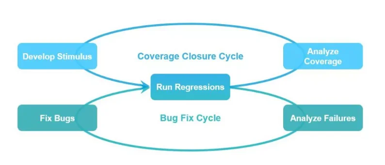
Figure 1: AI is most valuable where verification teams repeatedly lose time in debugging, regression analysis, and coverage-closure efforts.
Source: [Synopsys]
In semiconductor verification, AI creates value first by reducing friction in the most repetitive loops. This includes debugging, regression analysis, and coverage closure, which engineers traditionally spend a significant portion of their project time on. That contribution is fundamentally different from replacing engineers, who define what to verify, interpret evidence, and decide when residual risk is acceptable [2].
What Skills Do Semiconductor Engineers Need to Use AI Effectively?
The engineers who gain most from AI will not be those who simply use generic AI tools. They will be the engineers who understand where AI can safely reduce effort, where outputs need review, and where engineering judgement must remain in control. In semiconductor work, AI is only useful when it is connected to design intent, verification evidence, manufacturing constraints and programme risk.
The most important skills are therefore a combination of semiconductor domain knowledge, automation capability and review discipline.
| Skill area | Why it matters in AI-assisted semiconductor engineering |
| Verification strategy | AI can help with regression triage, log analysis and coverage investigation, but engineers still define what must be verified and what evidence is meaningful. |
| Data interpretation | Semiconductor teams work with logs, coverage data, timing reports, yield data, process data and defect patterns. AI outputs are only useful when engineers can interpret the data behind them. |
| Scripting and automation | Python, Tcl, shell scripting, CI workflows and EDA automation remain practical foundations for using AI inside real engineering flows. |
| Machine learning basics | Engineers do not need to become AI researchers, but they should understand training data, model limits, validation, bias, confidence and failure modes. |
| Prompt and review discipline | AI-generated summaries, scripts, tests or documentation must be checked against specifications, constraints and engineering intent. |
| System-level trade-off judgement | AI can suggest options, but engineers still balance power, performance, area, cost, schedule, reliability, manufacturability and risk. |
| Governance and traceability | In production semiconductor programmes, teams need reviewable outputs, clear ownership, version control and evidence that can support sign-off decisions. |
This is why the future semiconductor engineer is not simply an AI user. The stronger role is closer to an AI supervisor inside a controlled engineering process. Engineers must know how to frame the problem, provide the right context, challenge AI-generated outputs and decide whether the result is technically safe to use.
For verification teams, this is especially important. AI can reduce time spent searching logs, grouping failures or summarising regression results, but it does not decide whether the verification plan is complete. It does not know whether a coverage target reflects real functional intent. It does not own the decision that a design is ready for sign-off. That responsibility remains with engineers [2], [3], [7].
This makes skills development a management issue as well as an individual learning issue. Organisations adopting AI in semiconductor engineering need to train engineers not only to use tools, but to apply AI within disciplined design, verification and manufacturing workflows.
How Can Semiconductor Engineers Learn AI and Machine Learning?
Semiconductor engineers do not need to become full-time machine learning researchers to benefit from AI. The more valuable goal is to understand enough AI and machine learning to use these methods responsibly inside engineering workflows.
A practical learning path should begin with the engineering problem, not the tool. Engineers should first identify where time is being lost. This could include regression debug, log review, documentation search, coverage analysis, design-rule checking, yield investigation or manufacturing anomaly detection. Once the problem is clear, AI can be assessed as a support method rather than treated as a general solution.
| Learning area | Practical relevance for semiconductor engineers |
| Python and data analysis | Useful for handling logs, reports, coverage exports, yield data and engineering metrics. |
| Statistics and probability | Helps engineers understand variation, confidence, anomaly detection and measurement uncertainty. |
| Machine learning fundamentals | Provides a foundation for classification, clustering, prediction and model validation. |
| EDA workflow automation | Connects AI support to real design, verification and implementation flows. |
| Prompt engineering and review | Helps engineers get better AI outputs while maintaining technical control. |
| Verification and sign-off discipline | Ensures AI-assisted work remains connected to specifications, evidence and accountability. |
| Data governance | Protects sensitive IP, design data, customer information and project-specific engineering knowledge. |
The safest approach is to learn through bounded use cases. For example, a verification engineer could begin by using AI to summarise regression logs, group similar failures or retrieve methodology guidance. A design engineer could use AI to support documentation search, script generation or design-space exploration. A manufacturing engineer could use AI to explore defect patterns, process trends or yield anomalies.
However, every learning path should include a review step. AI-generated results should be compared with known data, checked by engineers and measured against baseline performance. This prevents teams from treating AI output as authority simply because it is fast or well presented.
The goal is not to replace engineering judgement with AI judgement. The goal is to help engineers move faster through repetitive or data-heavy tasks while preserving technical ownership of the decision.
Why AI Verification Still Depends on Human Engineering Intent
Verification is where the replacement argument becomes weakest. AI can help with regression triage, pattern recognition, failure clustering, parts of debugging, and selected coverage-closure work. Synopsys has clearly framed this for some time: AI can improve efficiency in the verification cycle and reduce wasted effort in debugging and analysis [2]. That matters because verification complexity continues to rise as designs grow into large SoCs, 3D-ICs, and multi-die systems [3].
What AI does not do is define verification intent. It does not decide whether the team is proving the right thing. It does not resolve ambiguity in requirements. It does not determine whether a coverage number represents meaningful evidence or merely activity. Semiconductor Engineering’s discussion of the evolving role of AI in verification is useful here because it explicitly frames AI as integrated with human expertise rather than as a replacement for it [3]. That distinction is critical in real projects. Verification is not only about producing tests. It is about deciding what the design must still demonstrate before a responsible team can sign it off.
The role of AI in verification also highlights the importance of the quality of context. Semiconductor Engineering has separately warned that generic LLM-based approaches can miss verification context, misunderstand code bases, and introduce hallucinations that are particularly dangerous in design verification work [7]. In other words, even where AI assists, the need for strong engineering review increases rather than disappears. Teams that want greater confidence in their decisions still need clear specifications, disciplined assumptions, and engineers who challenge outputs rather than accept them at face value.
That is why related Alpinum material, such as Verification Planning to Coverage Closure, remains relevant even in an AI discussion. Better tooling does not remove the need for a sound verification strategy.
Are Semiconductors Needed for AI?
Yes. AI depends heavily on semiconductors. Modern AI systems require advanced processors, AI accelerators, graphics processing units, high-bandwidth memory, networking chips, storage, power-management devices and advanced packaging technologies. Without semiconductor engineering, there is no scalable AI infrastructure.
This is one reason the question “will AI replace semiconductor engineers?” can be misleading. AI is increasing demand for the very hardware that semiconductor engineers design, verify and manufacture. Data-centre AI, edge AI, automotive AI, industrial automation and AI-enabled communications systems all depend on reliable semiconductor capability.
The impact is therefore circular. AI tools may support parts of chip design, verification and manufacturing, but AI growth also creates greater pressure on chip teams. More compute demand means more complex architectures, tighter power and performance constraints, more advanced packaging, more verification pressure and stronger manufacturing requirements.
This is why AI should not be viewed only as a labour replacement issue. In semiconductors, AI is both a tool used inside engineering workflows and a market force increasing demand for engineering capability. The more realistic 2026 picture is that AI raises the performance bar for semiconductor teams rather than removing the need for them.
For engineering leaders, the practical issue is how to build teams that can support this demand. That includes stronger design automation, better verification planning, more efficient debug flows, improved manufacturing analytics and clearer governance around AI-assisted outputs.
The Semiconductor Trade-Off Problem AI Does Not Own
Semiconductor engineering is not a single-objective exercise. Teams balance power, performance, area, cost, schedule, testability, reliability, safety, security, software implications, and manufacturability at the same time. A local improvement in one metric can create new problems somewhere else. That is why experienced engineers spend much of their time dealing with trade-offs rather than simply executing isolated tasks [4].
Design News captures this broader engineering problem well. It argues that engineering decisions involve interpretation, unstated assumptions, and the balancing of tangible and intangible requirements. Real projects do not present themselves as clean textbook exercises [6]. That observation applies even more strongly in semiconductors, where design decisions often propagate across abstraction levels and teams. A timing fix can affect verification effort. A packaging decision can affect thermal behaviour. A power optimisation can shift software or validation complexity. AI can help surface options more quickly, but it does not make the trade-off between them [6].
The reported Apple–Intel foundry deal also reflects how AI competition is shifting attention towards semiconductor manufacturing capacity and long-term supply-chain resilience.
Semiconductor Manufacturing Will Use More AI, Not Fewer Engineers
The same pattern appears in manufacturing. AI is becoming more useful in semiconductor manufacturing because fabs and manufacturing operations generate vast quantities of data that are difficult to interpret manually at speed. Siemens’ recent article on semiconductor manufacturing frames this as a move towards industrial AI, digital twins, and data-driven operational decision-making [5]. That is a meaningful shift in capability. It can improve anomaly detection, what-if analysis, process understanding, and the speed with which teams move from raw data to operational insight.
Siemens also makes an important point about domain specificity. In semiconductor manufacturing, models need to understand what matters to engineers and operators, including accuracy, speed, and safety. Breadth alone is not enough [5]. Siemens’ analysis highlights that manufacturing AI becomes useful only when grounded in a domain context. A fab does not need general intelligence in the abstract. It needs tools that support better operational decisions in a very specific environment.
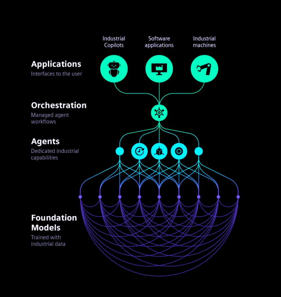
Figure 2: Semiconductor manufacturing benefits from AI when models are tied to engineering context, operational constraints, and decision quality. Source: [Siemens]
The value comes from combining models, workflows, and domain expertise to help engineers make better decisions more quickly [5].
How Engineers Can Learn AI for Semiconductor Manufacturing
AI in semiconductor manufacturing is not the same as generic machine learning applied to ordinary business data. Semiconductor manufacturing involves high-value assets, sensitive process windows, complex equipment behaviour, yield dependencies, inspection data, metrology results and strict quality expectations. An AI model is only useful when it supports decisions inside that operational context.
Engineers who want to apply AI in semiconductor manufacturing should begin with the data sources that already shape manufacturing decisions. These may include process logs, metrology data, wafer inspection results, equipment sensor data, defect maps, yield records and maintenance history. AI can help detect patterns in these datasets, but engineers still need to understand which patterns are meaningful and which may be misleading.
A practical learning path for manufacturing engineers should include five stages.
| Stage | Learning focus | Practical outcome |
| 1. Build data foundations | Python, data cleaning, visualisation and statistical analysis | Engineers can inspect manufacturing data before applying AI. |
| 2. Understand semiconductor data sources | Process logs, metrology, inspection, yield and equipment data | AI work remains grounded in fab realities. |
| 3. Learn core AI methods | Classification, clustering, anomaly detection and predictive modelling | Engineers can match AI methods to manufacturing problems. |
| 4. Connect AI to decisions | Yield improvement, defect investigation, equipment monitoring and process control | AI supports engineering action, not just dashboard reporting. |
| 5. Validate and govern outputs | Model testing, traceability, review and operational risk control | AI recommendations can be assessed safely before use. |
This matters because manufacturing decisions carry real operational consequences. A model may identify a process anomaly, but engineers still need to decide whether it reflects equipment drift, material variation, measurement noise, process instability or a broader production issue. AI can shorten the path from data to insight, but it cannot remove the need for domain interpretation.
The strongest manufacturing use cases are likely to be those where AI helps engineers see patterns faster. These include defect classification, yield analysis, predictive maintenance, process window monitoring, and digital twin support. In each case, the benefit comes from combining AI with engineering context, not from treating AI as an independent decision-maker [5].
For semiconductor leaders, this creates a clear training requirement. Manufacturing engineers need AI literacy, but they also need workflows that make AI outputs reviewable, traceable and connected to production risk.
AI in Chip Design, Verification and Manufacturing: Where Engineers Still Matter
AI affects different parts of semiconductor engineering in different ways. It can reduce manual effort in some areas, improve access to information and help teams identify patterns more quickly. However, the most important decisions still require engineering ownership.
| Engineering area | What AI can support | What engineers still own |
| Chip design | Documentation search, code assistance, optimisation support, script generation and design-space exploration | Architecture, constraints, trade-offs, review quality and accountability |
| Design verification | Regression triage, log summarisation, failure clustering, debug support and coverage investigation | Verification intent, specification interpretation, coverage meaning, risk judgement and sign-off confidence |
| Semiconductor manufacturing | Defect analysis, yield modelling, anomaly detection, equipment monitoring and digital twin support | Process interpretation, operational decisions, safety, quality and production risk |
| Engineering management | Workflow automation, reporting, knowledge retrieval and productivity tracking | Capability planning, governance, project risk, training and adoption strategy |
| AI adoption strategy | Tool comparison, pilot support, data analysis and workflow recommendations | Use-case selection, success metrics, IP protection, review process and deployment control |
This distinction is important because semiconductor engineering is not a collection of isolated tasks. A design change can affect verification. A verification gap can affect schedule risk. A packaging decision can affect thermal behaviour. A manufacturing issue can expose design or process assumptions. AI can help teams move faster inside parts of this system, but it does not replace the system-level judgement needed to manage the whole programme.
For this reason, the most effective use of AI in semiconductors will be selective and measured. Teams should start with bounded problems where outputs can be reviewed, baselines can be measured and risk can be controlled. Examples include regression triage, debug assistance, documentation retrieval, coverage investigation and manufacturing data analysis.
The weaker approach is to treat AI as a general replacement for engineering expertise. That creates the risk of faster outputs without stronger evidence. In semiconductor programmes, speed only matters when it improves decision quality, reduces avoidable rework and supports responsible sign-off.
What Will Change for Semiconductor Engineers in 2026
The most likely workforce effect is not wholesale displacement. It is a combination of task displacement and role elevation. Repetitive work will continue to shrink. Engineers who can use AI effectively will gain a competitive advantage. Engineers who can supervise AI-assisted workflows, validate outputs, and make cross-domain decisions will become more valuable, not less.[1][4]
This conclusion also fits the industry’s broader labour picture. SEMI reports that by 2030, the semiconductor industry will need to add 1 million skilled workers globally, with shortages of over 100,000 engineers in Europe and more than 200,000 engineers in Asia-Pacific [8]. That is not a signal of collapsing engineering demand. It is a signal that the industry still needs more talent, while the content of the work is changing.
The more serious management question concerns the learning path. If organisations automate too much routine work without redesigning how junior engineers learn, they may weaken the future pipeline that produces strong architects, verification leads, and manufacturing specialists. AI can improve throughput, but it does not remove the need to build engineering judgement. For that reason, capability development remains central. Alpinum’s Training and Formal Verification resources are relevant next steps for teams thinking about how skills must evolve alongside tooling.
Semiconductor Engineering Outlook 2026: AI Demand Raises the Skills Bar
The 2026 outlook for semiconductor engineering is not a collapse in demand. It is a shift in capability expectations. AI chips, data-centre infrastructure, advanced packaging, verification complexity and manufacturing automation all require engineers who can combine semiconductor domain expertise with AI-assisted workflows.
This means the strongest teams will not be those that simply adopt AI tools. They will be the teams that integrate AI into controlled engineering processes. That includes clear use-case selection, measurable baselines, secure data handling, review steps, traceability and defined ownership of final decisions.
For chip design teams, the pressure will be on faster exploration, better automation and stronger review of AI-assisted outputs. For verification teams, the pressure will be on reducing debug and regression friction while preserving verification intent and sign-off confidence. For manufacturing teams, the pressure will be on using data more effectively without weakening operational judgement.
This is why AI adoption should be treated as an engineering capability programme rather than a software procurement exercise. The question is not only which AI tools a team can access. The more important question is whether the organisation has the skills, data, process maturity and governance needed to use AI safely in production semiconductor work.
In this context, AI is likely to increase the value of engineers who can work across domains. Engineers who understand both semiconductor constraints and AI-assisted workflows will be better placed to manage future design, verification and manufacturing challenges.
Conclusion: AI Will Reshape Semiconductor Engineering Roles, Not Remove Accountability
So, will AI replace engineers in the semiconductor industry? No, not in the way the question is usually asked.
AI will replace some tasks. It will reduce manual effort in documentation-heavy work, parts of debugging, selected optimisation loops, and manufacturing analytics. It will also raise expectations for productivity and make weak workflows more visible. But semiconductor development still depends on human ownership of intent, trade-offs, review quality, and sign-off accountability. AI will make strong engineers more effective. It will reward teams that combine automation with sound engineering discipline. It will not remove the need for people to define what the system must do, judge whether the available evidence is sufficient, and take responsibility for decisions when the cost of error is high.
Organisations exploring the role of AI in semiconductor engineering must consider not only the tooling but also how AI integrates with existing design, verification, and manufacturing workflows.
Alpinum Consulting supports engineering teams in applying AI within structured, production-ready environments, with a focus on decision confidence, verification integrity, and system-level outcomes.
FAQ – Will AI Replace Semiconductor Engineers?
Will AI replace semiconductor engineers?
No. AI is more likely to replace selected repetitive tasks than full semiconductor engineering roles. Engineers are still needed to define intent, manage design constraints, review results, judge risk and take responsibility for sign-off decisions.
Which semiconductor engineering tasks can AI automate?
AI can help with documentation search, code assistance, log summarisation, regression triage, debug support, design-rule checking, routine optimisation and manufacturing data analysis.
Why can’t AI fully replace verification engineers?
Verification depends on intent, specification quality, coverage meaning, risk judgement and sign-off confidence. AI can support these activities, but it cannot independently decide whether the team is proving the right thing.
Will AI reduce the number of chip design jobs?
AI may reduce manual effort in some tasks, but the semiconductor industry still faces strong demand for skilled engineers. The bigger change is likely to be role evolution, with more emphasis on AI-assisted workflows, review discipline and cross-domain decision-making.
What skills should semiconductor engineers learn for AI-era workflows?
Engineers should strengthen skills in verification strategy, prompt and review discipline, data interpretation, EDA automation, scripting, AI-assisted debug, coverage analysis and system-level trade-off decisions.
What skills do semiconductor engineers need for AI?
Semiconductor engineers need skills in verification strategy, data analysis, scripting, EDA automation, machine learning basics, prompt review, governance and system-level engineering judgement. The most valuable engineers will be those who can use AI to reduce repetitive effort while still checking outputs against specifications, constraints and sign-off requirements.
How can semiconductor engineers learn AI and machine learning?
Semiconductor engineers can start with Python, data analysis, statistics and machine learning fundamentals. They should then apply those skills to practical semiconductor use cases such as regression analysis, log summarisation, coverage investigation, design automation, yield analysis or manufacturing anomaly detection.
How can engineers learn AI for semiconductor manufacturing?
Engineers should focus on semiconductor manufacturing data first. This includes process logs, metrology data, inspection data, yield records, equipment sensor data and defect patterns. They can then learn AI methods such as classification, clustering, anomaly detection and predictive modelling, while keeping engineering review and process knowledge central.
Are semiconductors needed for AI?
Yes. AI depends on advanced semiconductors, including GPUs, AI accelerators, high-bandwidth memory, networking chips, storage, power devices and advanced packaging. AI growth increases demand for semiconductor design, verification and manufacturing capability.
Will AI replace semiconductor manufacturing engineers?
AI will automate parts of monitoring, analysis and optimisation, but it is unlikely to replace semiconductor manufacturing engineers. Engineers are still needed to interpret process behaviour, manage quality, understand operational risk and make production decisions.
Will AI replace chip design engineers?
AI can support chip design engineers with documentation search, code assistance, optimisation, design-space exploration and repetitive flow tasks. However, engineers still own architecture, constraints, trade-offs, review and accountability.
Why is AI adoption in semiconductor engineering risky without governance?
AI adoption is risky without governance because semiconductor work involves sensitive IP, complex design context, safety considerations and high-cost errors. Teams need clear rules for data use, output review, traceability, accountability and sign-off before AI can be used safely in production workflows.
Continue Exploring
- AI adoption in design verification
Explore how engineering teams can adopt AI in DV with clearer governance, measurable pilots and reviewable workflows. - Design and verification capability
Review Alpinum’s design verification support for teams managing complex semiconductor development and verification risk. - Formal verification for sign-off confidence
See how formal verification supports stronger evidence, deeper bug analysis and higher sign-off confidence.
For additional technical context, the following insight extends the themes discussed in this article:
System-scale programme risk in verification
References
[1] S. Krishnamoorthy, “How AI is Supercharging Chip Design Workflows,” Synopsys Blog, Oct. 23, 2025. [Online].
Available:https://www.synopsys.com/blogs/chip-design/ai-chip-design-workflow-automation.html.
[2] Synopsys, “SoC Design Verification and Chip Debug with AI,” Synopsys Blog, Mar. 22, 2023. [Online].
Available: https://www.synopsys.com/blogs/chip-design/ai-soc-design-verification-flow.html.
[3] A. Mutschler, “The Evolving Role Of AI In Verification,” Semiconductor Engineering, Mar. 26, 2025. [Online].
Available: https://semiengineering.com/the-evolving-role-of-ai-in-verification/.
[4] E. Sperling, “How AI Will Impact Chip Design And Designers,” Semiconductor Engineering, Jul. 31, 2025. [Online].
Available: https://semiengineering.com/how-ai-will-impact-chip-design-and-designers/.
[5] Calibre IC Design & Manufacturing, “From data to domain expertise: How AI, accelerated computing and digital twins are reshaping semiconductor manufacturing,” Siemens Digital Industries Software Blog, Mar. 20, 2026. [Online].
[6] P. Parendo, “Will AI Replace Engineers?” Design News, Jan. 14, 2026. [Online].
Available: https://www.designnews.com/artificial-intelligence/will-ai-replace-engineers.
[7] “The Limits Of AI’s Role In EDA Tools,” Semiconductor Engineering, Sep. 25, 2025. [Online]. Available: https://semiengineering.com/the-limits-of-ais-role-in-eda-tools/.
[8] J.-B. Smits, “The Semiconductor Talent Crisis: Why Growing Demand Can’t Find Leaders,” SEMI, Jun. 23, 2025. [Online].
Available: https://www.semi.org/en/blogs/the-semiconductor-talent-crisis-why-growing-demand-cant-find-leaders.
[9] Synopsys, “Generative and Agentic AI in Chip Design Explained,” Feb. 2026.
[10] Siemens, “Siemens & TSMC to advance AI for semiconductor design,” Apr. 2026.

Written by : Mike Bartley
Mike started in software testing in 1988 after completing a PhD in Math, moving to semiconductor Design Verification (DV) in 1994, verifying designs (on Silicon and FPGA) going into commercial and safety-related sectors such as mobile phones, automotive, comms, cloud/data servers, and Artificial Intelligence. Mike built and managed state-of-the-art DV teams inside several companies, specialising in CPU verification.
Mike founded and grew a DV services company to 450+ engineers globally, successfully delivering services and solutions to over 50+ clients.
Mike started Alpinum in April 2016 to deliver a range of start-of-the art industry solutions:
Alpinum AI provides tools and automations using Artificial Intelligence to help companies reduce development costs (by up to 90%!) Alpinum Services provides RTL to GDS VLSI services from nearshore and offshore centres in Vietnam, India, Egypt, Eastern Europe, Mexico and Costa Rica. Alpinum Consulting also provides strategic board level consultancy services, helping companies to grow. Alpinum training department provides self-paced, fully online training in System Verilog, UVM Introduction and Advanced, Formal Verification, DV methodologies for SV, UVM, VHDL and OSVVM and CPU/RISC-V. Alpinum Events organises a number of free-to-attend industry events
You can contact Mike (mike@alpinumconsulting.com or +44 7796 307958) or book a meeting with Mike using Calendly (https://calendly.com/mike-alpinum-consulting).
Stay Informed and Stay Ahead
Latest Articles, Guides and News
Explore related insights from Alpinum that dive deeper into design verification challenges, practical solutions, and expert perspectives from across the global engineering landscape.