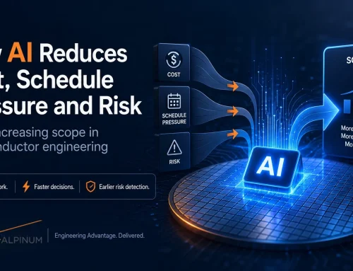
Artificial intelligence is moving from experimental engineering support into production semiconductor design flows. For chip teams, this shift is especially important because modern semiconductor development is becoming more complex, schedule-sensitive and verification-intensive.
AI agents in chip design are now being explored for tasks such as specification interpretation, RTL support, verification planning, testbench generation, regression analysis, debug assistance and workflow orchestration [1][2][3]. These are not abstract use cases. They sit directly in the areas where design and verification teams often face schedule pressure, engineering bottlenecks and repeated manual effort.
This topic forms part of the wider Verification Futures 2026 discussion, in which semiconductor engineering leaders are examining how AI, verification complexity, chiplet-based systems and production design flows are changing the direction of advanced technology programmes.
| Key learning point | Link to detailed explanation | External reference link |
| AI agents are moving from experimental assistants into production chip design workflows | Why AI Agents Matter for Chip Teams | [1], [3] |
| Verification planning, testbench generation, regression analysis, and debugging are practical early use cases | Where AI Agents Can Support Design and Verification | [2], [3] |
| Production deployment requires accuracy, traceability and human review | The Challenge of Trust, Reliability and Sign-Off Confidence | [3], [4] |
| Agentic AI depends on a strong engineering context, data quality and integration with existing EDA flows | Infrastructure, Data and Workflow Integration | [4], [5] |
| The strongest adoption path is controlled pilots rather than uncontrolled automation | What Semiconductor Teams Should Do Next | [6] |
About the Speaker: Kartik Hegde
| Kartik Hegde is Senior Group Director of Agentic AI and ChipStack at Cadence Design Systems. He joined Cadence following the acquisition of ChipStack, an AI-driven chip design startup that he co-founded and led as CEO.His background combines computer architecture, machine learning and practical semiconductor engineering. He completed his PhD in Computer Science at the University of Illinois Urbana-Champaign, where his research focused on the intersection of computer architecture and machine learning. He has also worked on high-performance processors for machine learning workloads and AI tools designed to improve computing efficiency [1][2].This combination of research, startup execution, and production EDA experience makes him well-placed to discuss how AI agents can be used by real chip teams, not just as demonstrations but as practical tools within semiconductor design and verification flows. |  Image Source: Tessolve |
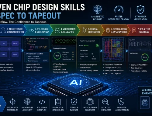
Why AI Agents Matter for Chip Teams
Modern chip development involves a growing number of specifications, design blocks, verification environments, scripts, regressions, documentation sources and sign-off requirements. As semiconductor programmes become more complex, teams spend significant effort understanding design intent, writing and reviewing code, building verification plans, generating tests, debugging failures and coordinating across multiple tools.
This is where AI agents are becoming relevant. Unlike simple chat-based assistants, AI agents are designed to work across tasks, tools and workflows. In a chip design context, they can help interpret specifications, reason about design behaviour, suggest verification strategies, generate or refine code, analyse logs and support iterative debugging [3][4].
For production chip teams, the value is not only speed. The more important question is whether AI can reduce repetitive engineering effort while preserving quality, traceability and sign-off confidence. Chip design cannot tolerate uncontrolled automation. A generated test, assertion, script or RTL change must be explainable, reviewable and compatible with the wider engineering flow.
This is why Kartik Hegde’s topic is important. It moves the discussion away from general AI enthusiasm and towards practical deployment: where AI agents work, where they fail, what infrastructure they require and how teams can build trust in production use cases.
Where AI Agents Can Support Design and Verification
AI agents can support several parts of the chip design and verification lifecycle. One early area is specification analysis. Engineers often need to understand large design documents, protocol requirements, interface descriptions and system constraints before writing RTL or planning verification. An AI agent can help summarise requirements, identify dependencies and connect specification details to design or verification tasks.
A second area is verification planning. Verification teams need to convert design intent into test objectives, coverage goals, assertions and regression strategies. AI agents may help draft initial verification plans, suggest missing scenarios, map requirements to test cases and identify areas where coverage needs stronger justification [3][5].
A third area is debugging. Regression failures often require engineers to inspect logs, waveforms, error messages, configuration files and recent design changes. AI agents can help triage failures, identify patterns, summarise likely root causes and suggest next debugging steps. This does not remove the need for engineering judgement, but it can reduce the time spent on repetitive investigation.
A fourth area is testbench and script support. AI agents may help generate testbench components, automate boilerplate, update scripts and assist with routine flow maintenance. These tasks are often time-consuming but still require careful review to avoid subtle errors.
The strongest production use cases are therefore likely to be those in which AI augments engineering judgement rather than replaces it. In design verification, this means using AI to accelerate planning, analysis and debugging while keeping human engineers responsible for decisions that affect correctness, coverage and sign-off.
The Challenge of Trust, Reliability and Sign-Off Confidence
The main barrier to AI agents in production chip teams is not whether they can generate useful output. The harder question is whether the output can be trusted.
Chip design and verification are high-consequence engineering activities. A missed bug can become expensive after tape-out, and a poorly understood automation step can create hidden risk. This makes AI adoption different from general software productivity use cases. Semiconductor teams need explainability, version control, audit trails, verification evidence and clear ownership of decisions [4][6].
AI agents can also make mistakes. They may misunderstand the design intent, overgeneralise from an incomplete context, generate plausible but incorrect code, or recommend a debugging path that misses the root cause. In production workflows, these risks must be controlled through guardrails, human review and integration with deterministic verification tools.
A practical AI agent for chip teams, therefore, needs more than a language model. It needs access to the right engineering context, such as specifications, RTL, verification plans, regression results, design hierarchy and tool outputs. It also needs to operate inside a controlled workflow where engineers can inspect what was changed, why it was changed and how the result was validated.
This is why sign-off confidence remains central. AI can help accelerate work, but it cannot replace the discipline of verification, closure, coverage analysis and engineering accountability.
Infrastructure, Data and Workflow Integration
Deploying AI agents in production chip teams also raises infrastructure questions. Semiconductor workflows involve multiple EDA tools, file formats, data sources, abstraction levels and team-specific processes. An agent must be able to reason across this fragmented environment without breaking established flows.
The value of agentic AI depends heavily on context. If an AI agent only sees isolated text, it may produce generic suggestions. If it can access design structure, verification intent, past regressions, tool results and project-specific methodology, it can become much more useful. However, this also raises concerns about data quality, permissions, IP protection, security, and workflow governance [4][5].
Another issue is integration. Production teams rarely work in a single tool. They use simulation, formal verification, coverage analysis, lint, synthesis, CI pipelines, issue trackers and documentation systems. AI agents must fit into these environments rather than forcing teams to rebuild their entire flow.
This is why the best adoption model is likely to be incremental. Teams should begin with bounded use cases where the inputs, outputs, review steps and success metrics are clear. For example, an AI agent could first support regression triage, draft verification plan sections, or summarise specification changes before being trusted with more complex design-flow orchestration.
Other Experts Shaping AI Agents in Semiconductor Engineering
Paul Cunningham
| Paul Cunningham, Senior Vice President and General Manager of System Verification at Cadence, has been closely associated with the practical deployment of AI in EDA and verification workflows. His perspective is important because agentic AI must be grounded in the realities of production engineering, where accuracy and correctness are essential.Cadence’s work around ChipStack AI Super Agent has highlighted how AI agents may support front-end chip design and verification by building models of design intent, using EDA tools and assisting with bug detection and correction [3]. This reflects a broader industry trend towards AI-supported engineering workflows that augment human teams while preserving verification discipline. |  Image Source: cadence.com |
Key contribution: Cadence ChipStack AI Super Agent for chip design and verification [3].
Sassine Ghazi
| Sassine Ghazi, President and CEO of Synopsys, has discussed the progression from AI assistants towards agentic systems in semiconductor engineering. This includes the idea that AI-enabled workflows may evolve through stages, from task assistance to orchestration and eventually more autonomous decision-making across parts of the design flow [6].His perspective is relevant because it frames AI agents as part of a broader engineering transformation rather than a single tool category. For semiconductor teams, this means AI adoption will not be only about productivity. It will also affect workflow design, engineering roles, accountability and how teams manage complexity across increasingly demanding chip programmes. |  Image Source: synopsys.com |
Key contribution: Industry framing of agentic AI as the next wave of EDA automation and workflow orchestration [6].
Brian Bailey
| Brian Bailey, Technology Editor at Semiconductor Engineering, has written about the methodological challenges behind agentic EDA. His work highlights that agentic AI must reason across multiple tools, vendors, data formats and abstraction levels to become useful in real semiconductor flows [4].This perspective is valuable because it focuses on the gap between promising AI demonstrations and production deployment. Chip teams do not only need agents that can generate text or code. They need agents that understand context, methodology, tool constraints, design history and verification requirements. This makes workflow integration and data accessibility central to the future of agentic EDA. |  Image Source: x.com/brian_esl |
Key contribution: Analysis of the methodology, data and abstraction challenges behind agentic EDA [4].
What Semiconductor Teams Should Do Next
For teams exploring AI agents in chip design, the first step is to identify where repeated engineering effort creates measurable bottlenecks. Good starting points include drafting verification plans, regression triage, failure log summarisation, testbench boilerplate, and documentation search and review support.
The second step is to define control boundaries. AI should not be introduced as an uncontrolled layer over sign-off-critical work. Teams need clear review points, version control, tool integration, access permissions and measurable success criteria.
The third step is to run a safe pilot. A well-scoped pilot allows teams to test AI agents on a defined workflow, measure productivity impact, assess output quality and understand where human review remains essential. This is particularly important in design verification, where confidence depends on evidence, traceability and repeatable methodology.
Teams working on advanced semiconductor programmes should also consider how AI agents affect design verification, AI adoption and system-level engineering confidence. Alpinum’s expertise in design verification and AI in DV adoption can help engineering teams assess where AI creates practical opportunities and where governance, validation and sign-off discipline must remain central. For teams beginning this journey, a safe AI in design verification pilot can provide a practical first step before wider deployment.
Conclusion
AI agents are becoming a serious topic for production chip teams because they address real bottlenecks in design and verification. Their value will depend not on autonomy alone, but on how well they support engineers, integrate with EDA workflows and preserve sign-off confidence. The teams that adopt them carefully will be best placed to benefit from the next phase of AI-enabled semiconductor engineering.
Need to understand how AI agents could affect your verification strategy?
As AI agents move into chip design, verification, and debug workflows, engineering teams need more than faster automation. They need a controlled adoption strategy that protects correctness, traceability and sign-off confidence.
Alpinum helps semiconductor teams assess design verification capability, identify where AI can be introduced safely, and define practical adoption roadmaps for advanced engineering programmes.
Explore Alpinum’s AI in DV Adoption service or learn more about our Design Verification services.
References
[1] Tessolve, Kartik Hegde Speaker Page: AI Agents in Production With Chip Teams: Opportunities, Challenges, and Lessons Learned
[2] Kartik Hegde, Biography and Research Background
[3] Reuters, Cadence introduces an AI agent to speed up computer chip design, 2026
[4] Semiconductor Engineering, Creating Agentic EDA Methodologies, 2026
[5] arXiv, The Dawn of Agentic EDA: A Survey of Autonomous Digital Chip Design, 2025
[6] Synopsys, How AI is Supercharging Chip Design Workflows, 2025

Written by : Mike Bartley
Mike started in software testing in 1988 after completing a PhD in Math, moving to semiconductor Design Verification (DV) in 1994, verifying designs (on Silicon and FPGA) going into commercial and safety-related sectors such as mobile phones, automotive, comms, cloud/data servers, and Artificial Intelligence. Mike built and managed state-of-the-art DV teams inside several companies, specialising in CPU verification.
Mike founded and grew a DV services company to 450+ engineers globally, successfully delivering services and solutions to over 50+ clients.
Mike started Alpinum in April 2016 to deliver a range of start-of-the art industry solutions:
Alpinum AI provides tools and automations using Artificial Intelligence to help companies reduce development costs (by up to 90%!) Alpinum Services provides RTL to GDS VLSI services from nearshore and offshore centres in Vietnam, India, Egypt, Eastern Europe, Mexico and Costa Rica. Alpinum Consulting also provides strategic board level consultancy services, helping companies to grow. Alpinum training department provides self-paced, fully online training in System Verilog, UVM Introduction and Advanced, Formal Verification, DV methodologies for SV, UVM, VHDL and OSVVM and CPU/RISC-V. Alpinum Events organises a number of free-to-attend industry events
You can contact Mike (mike@alpinumconsulting.com or +44 7796 307958) or book a meeting with Mike using Calendly (https://calendly.com/mike-alpinum-consulting).
Stay Informed and Stay Ahead
Latest Articles, Guides and News
Explore related insights from Alpinum that dive deeper into design verification challenges, practical solutions, and expert perspectives from across the global engineering landscape.