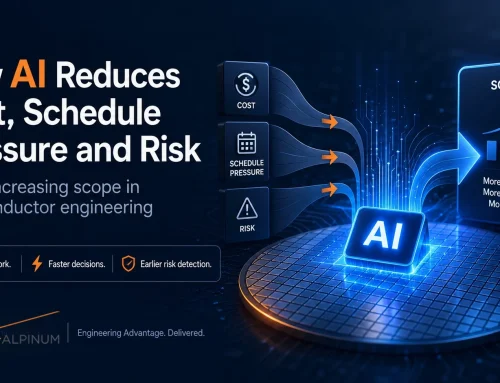
Artificial intelligence is changing the direction of semiconductor innovation. As AI models become larger, more complex and more energy-intensive, the industry can no longer rely only on traditional transistor scaling to deliver the next generation of compute performance [1].
This is where next-generation semiconductors become critical. The future of AI infrastructure will depend on specialised accelerators, advanced packaging, memory-centric architectures, chiplets, photonic computing, neuromorphic approaches and system-level co-design [2][3]. These trends are redefining compute beyond Moore’s Law and creating new opportunities across the semiconductor ecosystem.
This topic forms part of the wider Verification Futures 2026 discussion, in which semiconductor engineering leaders are examining how AI, chiplets, verification complexity, and system-level design are reshaping advanced technology programmes.
Five Key Learning Points
| Key learning point | Link to detailed explanation | External reference link |
| AI compute growth is pushing the industry beyond traditional Moore’s Law scaling | Why Next-Generation Semiconductors Matter for AI | [1] |
| Domain-specific accelerators are becoming central to AI training and inference workloads | Domain-Specific Accelerators and AI Hardware | [2] |
| Memory bandwidth, chiplets and advanced packaging are now major performance drivers | Memory, Chiplets and Advanced Packaging | [3], [4] |
| New compute architectures may reshape long-term AI semiconductor design | Beyond CPUs and GPUs: New Compute Architectures | [4], [5] |
| Energy efficiency and system-level co-design are now strategic priorities for AI infrastructure | Energy Efficiency Is Now a Strategic Constraint / System-Level Co-Design and the Future Semiconductor Roadmap | [5], [6] |
About the Speaker: Ekaterina Almasque
| Ekaterina Almasque is Managing Partner at BlankPage Capital and a recognised deep-tech investor focused on semiconductors, artificial intelligence, quantum computing and cybersecurity. She has backed and supported breakthrough technology companies across AI hardware and advanced computing, while serving on boards including IQM Quantum Computers, Hygraph, Binalyze and LatticeFlow.Her background combines venture leadership with a strong technical understanding of frontier technologies. This gives her a system-level perspective on how next-generation semiconductor innovation is evolving to support AI-driven workloads. Her experience across investment, emerging technologies, and scaling deep-tech companies makes her well-placed to discuss the future semiconductor roadmap for the AI era. |  Image Source: Tessolve |
Why Next-Generation Semiconductors Matter for AI
Artificial intelligence is reshaping semiconductor design at a pace not seen since the rise of mobile computing. Foundation models, large-scale training clusters and low-latency edge inference require enormous compute capacity. Traditional improvements driven by Moore’s Law and Dennard scaling are no longer sufficient on their own [1].
As a result, the semiconductor industry is moving towards architectural innovation rather than relying only on smaller process nodes. The focus is shifting from transistor density alone to performance per watt, memory bandwidth, system integration and workload-specific optimisation.
This marks a major change in how the industry thinks about compute. Instead of a single general-purpose processor for every use case, AI workloads increasingly require specialised architectures designed for parallel processing, efficient data movement, and software-hardware integration.
Domain-Specific Accelerators and AI Hardware
One of the most important trends in next-generation semiconductors is the rise of domain-specific accelerators. GPUs, tensor processors, AI ASICs and custom silicon are now central to the AI compute stack [2].
These architectures are designed to handle the parallelism required by machine learning workloads. In AI training and inference, performance depends not only on raw compute capacity but also on how efficiently data can move through the system. This is why specialised AI hardware has become increasingly important for data centres, edge devices and high-performance computing environments.
NVIDIA’s accelerated computing model is a strong example of how tightly coupled hardware and software ecosystems can improve performance per watt for AI systems [2]. Similar developments across the sector show how specialised hardware is replacing general-purpose architectures in performance-critical AI applications.
For semiconductor companies, this shift creates new design priorities. Engineers must consider workload behaviour, memory hierarchy, software frameworks, compiler support and verification complexity from the earliest stages of architecture planning.
Memory, Chiplets and Advanced Packaging
A second critical trend is memory-centric innovation. For advanced AI models, data movement can consume more energy than computation itself. This makes memory bandwidth and latency major constraints in AI system performance [3][4].
High-bandwidth memory, advanced packaging and chiplet architectures are emerging as key solutions. These technologies allow designers to bring compute and memory closer together, reduce bottlenecks and improve system-level performance.
Chiplets are particularly important because they allow different functions to be integrated into a single package without requiring every component to be manufactured on the same process node. This can improve flexibility, yield and cost efficiency while supporting more complex heterogeneous systems.
For readers looking at this trend from a practical engineering perspective, Alpinum has also explored why chiplets matter and how they are changing the economics, integration strategy and verification burden of modern semiconductor systems.
Advanced packaging is also becoming as important as transistor innovation. As conventional scaling becomes more difficult and expensive, packaging innovation provides another route to performance improvement. This is especially relevant for AI accelerators, where bandwidth, thermal performance and integration density can define the success of the final product.
Beyond CPUs and GPUs: New Compute Architectures
The future of AI semiconductors will not be limited to CPUs and GPUs. A third area of innovation involves entirely new compute architectures, including neuromorphic computing, photonic processors and in-memory computing.
Neuromorphic computing draws inspiration from the structure of biological neural systems, potentially enabling more efficient processing for certain AI workloads. Photonic computing explores the use of light for computation and data movement, which may help address bandwidth and energy limitations. In-memory computing seeks to reduce the cost of moving data by performing operations closer to where data is stored [4].
Many of these approaches remain early-stage, but they point to a broader redefinition of compute. As conventional architectures face economic, physical and energy constraints, the semiconductor industry is likely to explore a wider range of architectural options [4][5].
These technologies may not immediately replace today’s mainstream AI accelerators. However, they could become increasingly relevant as AI workloads continue to grow and as energy efficiency becomes a strategic constraint for data centres and edge systems [5][6].
Energy Efficiency Is Now a Strategic Constraint
Energy efficiency is no longer only an engineering concern. It is becoming a strategic limitation for AI infrastructure [5][6].
As AI data centres expand, power consumption, cooling requirements and sustainability pressures are becoming more important. Semiconductor innovation is therefore being measured not only by raw performance but also by the ability to deliver sustainable compute.
This has driven renewed interest in lower-power architectures, advanced cooling technologies, workload scheduling and system-level optimisation. For AI systems, the most successful semiconductor designs will be those that balance performance, scalability and energy efficiency.
This shift also affects design verification and validation. More complex architectures, multi-die integration and workload-specific optimisation increase the need for robust verification planning, hardware-software validation and system-level confidence before silicon delivery.
System-Level Co-Design and the Future Semiconductor Roadmap
Another important trend is system-level co-design. AI performance gains increasingly come from optimising the full stack rather than improving isolated hardware blocks [1][2].
Hardware, software, algorithms, compilers, memory systems and packaging must now be developed together. This changes the way semiconductor companies innovate. It also changes how engineering teams plan verification, validation and product delivery. This is also where AI adoption in DV becomes relevant. AI can support parts of planning, debugging, regression analysis and workflow optimisation, but it must be introduced with governance, traceability and sign-off discipline.
The future semiconductor roadmap is therefore unlikely to follow a single trajectory defined solely by process-node progression. Instead, it is becoming heterogeneous. The next phase of innovation will combine specialised accelerators, chiplet architectures, advanced packaging, memory innovation, software-hardware co-design and new materials.
This is the context in which next-generation semiconductors are becoming foundational to the AI era. They are opening opportunities not only for technical breakthroughs but also for new market leaders capable of solving compute, power and integration challenges at the system level [5][6].
Other Experts Shaping AI Semiconductor Innovation
Jensen Huang
| As founder and CEO of NVIDIA, Jensen Huang has helped define accelerated computing for AI. His contributions span GPU computing, CUDA ecosystems and AI infrastructure architecture. NVIDIA’s Hopper and Blackwell architectures show how specialised silicon and system-level integration can drive AI performance [2].Huang’s emphasis on full-stack optimisation, where hardware and software evolve together, has shaped the industry’s approach to scalable AI computing. Through GTC technical presentations and NVIDIA research initiatives, he has positioned accelerated computing as a central part of future semiconductor innovation [2]. |  Image Source: britannica.com |
Key contribution: NVIDIA Blackwell Architecture Technical Brief [2].
Jim Keller
| Jim Keller is one of the most influential chip architects in modern computing, known for processor design work at AMD, Apple, Tesla and Tenstorrent. His approach emphasises architectural efficiency, modularity and scalable compute design.This is particularly relevant as conventional semiconductor scaling slows. Keller has consistently highlighted that architectural innovation can continue to deliver performance improvements even when transistor scaling becomes more difficult. His work on AI-centric architectures and high-performance RISC-V processors provides an important perspective on how future compute systems may evolve [1]. |  Image Source: eetimes.com |
Key contribution: Introduction to Tenstorrent: Software, Silicon and Systems for AI.
Lisa Su
| As CEO of AMD, Lisa Su has driven major advances in heterogeneous computing and AI-focused processor design. Her work highlights how CPUs, GPUs and adaptive computing can be integrated to support demanding next-generation workloads.AMD’s technical contributions to advanced packaging, chiplets and accelerator development have become central to the semiconductor conversation. Su has also emphasised the need to balance performance, scalability and energy efficiency. These are critical priorities as AI systems place new pressure on compute infrastructure. |  Image Source: barrons.com |
Key contribution: ISSCC 2023 Keynote: Forging the Future of High-Performance Computing [4].
John Ternus
| John Ternus, Apple’s incoming CEO and current Senior Vice President of Hardware Engineering, represents an important industry perspective on next-generation semiconductors. Apple has announced that Tim Cook will transition to Executive Chairman, with Ternus becoming CEO from 1 September 2026 [7]. His leadership reflects the growing importance of custom silicon, system integration, and energy-efficient compute in modern product architectures.Ternus is particularly relevant because Apple’s semiconductor strategy is built on tight hardware-software co-design, advanced silicon integration and performance-per-watt optimisation. These priorities align closely with the broader industry shift towards AI-driven workloads, where system-level efficiency, custom architectures and integrated design approaches are becoming critical to future semiconductor innovation. |  Image Source: barrons.com |
Key contribution: Apple hardware engineering leadership across custom silicon-enabled products and AI-era system design strategy [7].
What Engineers and Semiconductor Teams Should Do Next
For those seeking deeper insight into next-generation semiconductors, several paths stand out. Technical research can be followed through IEEE publications, arXiv papers on AI hardware and conferences such as Hot Chips, ISSCC and DAC [3][4]. Industry roadmaps from the Semiconductor Industry Association also provide a broader context for long-term semiconductor trends [5].
A practical next step is to study the convergence of architecture, packaging and software co-design. These areas are becoming increasingly inseparable in AI systems. Emerging fields such as photonic computing, chiplets, energy-aware accelerators and memory-centric architectures also deserve close attention.
For engineers and verification professionals, engaging with these developments now is critical. Next-generation semiconductors will shape not only compute performance but also design methodologies, verification flows, system validation and commercial opportunities over the next decade.
Teams working on advanced semiconductor programmes should also consider how these trends affect design verification, AI adoption and system-level engineering confidence. Alpinum’s expertise in design verification and AI in DV adoption can help engineering teams assess where new technologies create practical opportunities and where careful governance, validation and sign-off discipline remain essential. For teams beginning this journey, a safe AI in design verification pilot can provide a practical first step before wider deployment.
Conclusion
The future of AI will not be determined by algorithms alone. It will also depend on semiconductor innovations that make those algorithms practical, scalable, and energy-efficient. As classical scaling reaches its limits, next-generation semiconductors are redefining compute through specialised architectures, advanced packaging and system-level thinking.
Need to understand how next-generation semiconductor trends affect your verification strategy?
As AI workloads, chiplets, advanced packaging and heterogeneous architectures reshape semiconductor design, engineering teams need more than faster tools. They need verification strategies that protect sign-off confidence while adapting to new system-level complexity.
Alpinum helps semiconductor teams assess design verification capability, identify where AI can be introduced safely, and define practical adoption roadmaps for advanced engineering programmes.
Explore Alpinum’s AI in DV Adoption service or learn more about our Design Verification services.
References
[1] Hennessy & Patterson, Computer Architecture: A Quantitative Approach
[2] NVIDIA Hopper Architecture Whitepaper, 2022
[3] Hot Chips Symposium Proceedings
[4] IEEE ISSCC Technical Papers
[5] Semiconductor Industry Association Roadmap
[6] McKinsey, The Future of AI Semiconductors
[7] Apple Newsroom, Tim Cook to become Apple Executive Chairman; John Ternus to become Apple CEO, 2026

Written by : Mike Bartley
Mike started in software testing in 1988 after completing a PhD in Math, moving to semiconductor Design Verification (DV) in 1994, verifying designs (on Silicon and FPGA) going into commercial and safety-related sectors such as mobile phones, automotive, comms, cloud/data servers, and Artificial Intelligence. Mike built and managed state-of-the-art DV teams inside several companies, specialising in CPU verification.
Mike founded and grew a DV services company to 450+ engineers globally, successfully delivering services and solutions to over 50+ clients.
Mike started Alpinum in April 2016 to deliver a range of start-of-the art industry solutions:
Alpinum AI provides tools and automations using Artificial Intelligence to help companies reduce development costs (by up to 90%!) Alpinum Services provides RTL to GDS VLSI services from nearshore and offshore centres in Vietnam, India, Egypt, Eastern Europe, Mexico and Costa Rica. Alpinum Consulting also provides strategic board level consultancy services, helping companies to grow. Alpinum training department provides self-paced, fully online training in System Verilog, UVM Introduction and Advanced, Formal Verification, DV methodologies for SV, UVM, VHDL and OSVVM and CPU/RISC-V. Alpinum Events organises a number of free-to-attend industry events
You can contact Mike (mike@alpinumconsulting.com or +44 7796 307958) or book a meeting with Mike using Calendly (https://calendly.com/mike-alpinum-consulting).
Stay Informed and Stay Ahead
Latest Articles, Guides and News
Explore related insights from Alpinum that dive deeper into design verification challenges, practical solutions, and expert perspectives from across the global engineering landscape.