
For decades, semiconductor engineering has operated within a hard delivery boundary. If a project increased in scope, it normally required more cost, more time, or more risk. If the schedule was compressed, the team usually needed more engineers, more automation, reduced scope, or higher residual risk. If cost was constrained, engineering leaders had to accept fewer features, less verification depth, longer delivery, or greater uncertainty.
The uncomfortable rule of semiconductor delivery has always been that cost, schedule, scope and risk cannot all move in the right direction at the same time.
AI is now beginning to change that.
AI does not remove the need for architecture judgement, design discipline, verification strategy, expert review or accountable sign-off. It does not make complex chip engineering easy. But it can reduce the internal pressure caused by repetitive manual work, late discovery, inefficient reuse, poor traceability, slow debugging, and incomplete visibility.
That is why AI in design verification matters. It can reduce costs, schedule pressure, and risk exposure while enabling delivery of a broader scope within the same engineering boundary.
The traditional trade-off: why all four dimensions rarely improve together
Traditional semiconductor delivery is constrained by four connected dimensions:
- Cost: engineering effort, EDA tools, compute resources, licences, IP, verification capacity, and specialist support.
- Schedule: time to requirements review, architecture freeze, RTL readiness, verification closure, physical design, embedded software readiness and sign-off.
- Scope: features, interfaces, protocols, power modes, performance targets, safety/security requirements and software-visible behaviour.
- Risk: functional bugs, missed requirements, weak coverage, integration failures, respins, late firmware issues and low sign-off confidence.
Historically, improving one dimension usually made another worse.
More scope meant more work. More work meant more cost, more time or more risk. A fixed tape-out date meant pressure on resource, scope or confidence. A fixed budget meant fewer engineers, less analysis, weaker reuse or delayed closure.
That is why simultaneously reducing cost, schedule pressure and risk whilst increasing scope was not a realistic claim. The internal area of the project was already full.
AI improves the delivery position within the engineering boundary
Figure 1 shows the traditional semiconductor delivery trade-off. In a conventional programme, improving one dimension usually increases pressure elsewhere. A faster schedule may require more engineering effort, reduced scope or higher delivery risk. A broader scope may require more cost, more time or greater uncertainty. Lower cost may reduce available engineering depth and increase sign-off risk.
The second panel shows the AI-enabled opportunity. AI does not remove engineering constraints, but it can reduce avoidable internal pressure by improving impact analysis, traceability, debug efficiency, knowledge reuse and earlier risk discovery. That creates the possibility of improving all four dimensions together: lower effort/cost, less schedule pressure, broader deliverable scope and lower delivery risk.
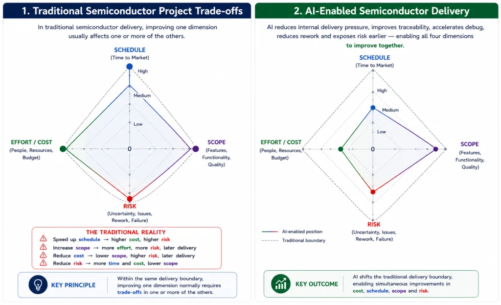
Figure 1: Traditional semiconductor delivery trade-off versus AI-enabled delivery improvement. AI does not remove engineering constraints; it reduces avoidable internal pressure so teams can improve schedule, effort/cost, scope and risk together.
AI changes the delivery equation by reducing the avoidable effort required to reach a defensible engineering outcome. The same programme may still face fixed team size, budget pressure, market windows and sign-off expectations. However, AI can reduce the pressure within those constraints by reducing repetitive searches, accelerating impact analysis, improving traceability, supporting regression triage, and exposing weak signals earlier.
That is why the AI-enabled position in Figure 1 can move in the right direction across all four dimensions. The improvement is not magic automation. It comes from reducing wasted effort and late discovery, allowing more engineering capacity to be used on useful scope, review quality and sign-off confidence.
The old boundary may remain the same: the same team size, the same budget pressure, the same market window, the same sign-off expectation. But AI can reduce the amount of internal area consumed by avoidable work.
For example, AI can help engineers:
- Compare specification versions and identify changed intent
- Summarise long design and verification documents
- Search previous bugs, decisions and known issue patterns
- Cluster regression failures and recurring debug signatures
- Identify affected tests, coverage points and documentation after a change
- Support first-pass requirements and verification-plan review
- Organise sign-off evidence and traceability
- Reduce repeated reporting and manual context reconstruction
AI does not remove the real engineering work. It reduces the waste around that work. If AI reduces the effective effort required for investigation, review, triage, reuse and planning, then the same project boundary can support more useful engineering scope.
| Engineering situation | Traditional impact | How AI reduces pressure | Resulting benefit |
| Late specification change | More manual review, more scheduling pressure, and a higher risk of missed impact. | AI helps compare specifications, identify changed intent and find affected tests, documents and coverage points. | Faster impact analysis and lower risk of missed dependencies. |
| Regression failures increase | Engineers spend more time reading logs and repeating debug investigations. | AI clusters similar failures, summarises logs and highlights recurring patterns. | Reduced debug effort and faster root-cause direction. |
| Requirements are ambiguous | Rework increases, and defects may be discovered late. | AI helps flag unclear wording, missing acceptance criteria and inconsistent documentation. | Earlier clarification and reduced late-stage risk. |
| Verification evidence is fragmented | Sign-off confidence becomes harder to defend. | AI helps organise links between requirements, tests, coverage, bugs and review evidence. | Stronger traceability and clearer sign-off readiness. |
| Project knowledge is spread across documents | Engineers waste time searching for previous decisions and known issues. | AI improves knowledge retrieval across specifications, bug history and project documentation. | Lower engineering cost and faster onboarding. |
| Scope increases but team size remains fixed | More scope normally means more cost, more time or more risk. | AI reduces avoidable work around analysis, triage, search, reuse and reporting. | More deliverable scope within the same engineering boundary. |
Table 1: How AI Reduces Cost, Schedule Pressure and Risk whilst Increasing Deliverable Scope
How AI reduces cost
AI reduces cost when it reduces avoidable engineering effort.
In semiconductor projects, cost is not only budget. It is also the time engineers spend searching for information, repeating previous analysis, reviewing long documents, debugging similar failures, recreating project context and manually preparing status evidence.
AI can reduce that wasted effort by improving access to engineering knowledge. A verification engineer can find related requirements, previous failures, test history, and coverage intent more quickly. A project leader can see repeated blockers earlier. A design team can compare specification changes without having to manually read every document from the beginning.
The saving is not that AI replaces expert engineers. The saving is that expert engineers spend less time reconstructing context and more time making technical decisions. AI-driven cost reduction becomes most useful when connected to disciplined design verification services, rather than treated as a generic automation tool.
How AI reduces schedule pressure
AI reduces schedule pressure by shortening feedback loops. Many semiconductor delays are caused by late visibility. A requirement ambiguity is discovered late. A coverage gap appears after repeated regressions. A firmware assumption is not verified against hardware behaviour until product validation. A small specification change affects more blocks than expected, but the true impact is not visible quickly enough.
AI can reduce the time between problem creation and problem discovery. It can support faster impact analysis, earlier triage, quicker log summarisation, better failure clustering and more efficient document review. Early discovery matters because an issue found early is easier to manage. The same issue found near sign-off becomes a schedule risk.
The benefit is not simply speed. The benefit is reduced decision latency. Reduced decision latency directly supports stronger verification planning and coverage closure, where early visibility and traceability are essential.
How AI reduces risk
AI reduces risk by exposing weak signals earlier and connecting them to evidence. In verification and semiconductor delivery, risk is not only the chance that a problem exists. It is also the chance that the team discovers it too late. AI can help reduce risk exposure by highlighting ambiguous requirements, recurring failure patterns, thin evidence of coverage, missing acceptance criteria, inconsistent documentation, and weak traceability.
However, AI only reduces risk when its output is reviewable. A generated test is not automatically useful. A generated summary is not proof. A suggested root cause is the lack of evidence of sign-off. AI must support engineering judgement, not bypass it.
The strongest AI use cases are therefore bounded and evidence-led: regression triage, log summarisation, requirements review, coverage gap analysis, verification planning support, debug evidence organisation and sign-off traceability. The need for measurable, reviewable AI adoption is why a structured “AI in DV” adoption assessment is more useful than adopting tools without first understanding verification maturity, review ownership and measurable engineering outcomes.
How AI enables increased scope
The key point is that AI does not make new scope free. A new protocol, safety requirement, power mode, performance target, or customer-specific feature still requires architecture, RTL, verification, software, validation and review. But AI can reduce the cost of understanding and managing the change. When a scope change occurs, AI can help identify affected documents, tests, coverage points, firmware assumptions, historical bugs, verification assets, and review items. Engineers still make the decision, but they start with better visibility.
Better visibility changes the practical boundary for delivery. If less effort is consumed by search, duplication, late discovery and manual triage, more effort is available for real engineering scope. AI can therefore support what was previously impossible: reducing cost, reducing schedule pressure and reducing risk whilst increasing the delivered scope.
The same principle applies across multiple semiconductor workflows. In formal verification, AI can help organise assumptions and documentation, but expert interpretation remains essential. In FPGA engineering and verification, AI can help reduce friction in prototype debugging and hardware/software investigation time. In embedded software testing, AI can support test evidence organisation, issue triage and hardware/software integration visibility.
The right way to measure AI in semiconductor engineering
AI adoption should not be measured by how much content, code or documentation it generates. It should be measured by its ability to reduce pressure.
Useful measures include:
- Less repeated debug effort
- Faster impact analysis after specification changes
- Earlier identification of coverage gaps
- Fewer missed assumptions
- Stronger traceability between requirements and verification evidence
- Faster access to project knowledge
- Higher-confidence reuse of previous assets
- Clearer sign-off evidence
The question is not: “Did AI generate more?” The question is: “Did AI reduce avoidable cost, schedule pressure or risk exposure, while enabling the team to deliver more useful scope?”
For teams building internal capability, AI adoption should also connect to practical semiconductor verification training. Engineers need the underlying skills to review AI output, challenge assumptions and connect suggestions back to real verification evidence. Strong review skills are especially important for teams working with RISC-V verification training, SV/UVM design verification training and advanced verification methodology.
The Alpinum view
The semiconductor industry does not need generic AI excitement. It needs disciplined AI adoption that respects engineering complexity. AI should not replace ownership, weaken sign-off evidence or hide uncertainty behind polished output. It should help engineering teams reduce avoidable work, expose risk earlier, strengthen review quality and make better use of existing knowledge.
The strongest use of AI is not to pretend that the cost–schedule–scope–risk rule no longer exists. The strongest use of AI is to reduce the internal pressure created by that rule. That is the real opportunity for semiconductor engineering: the old boundary remains, but AI reduces the internal area consumed by cost, schedule pressure and risk. That creates room for increased scope without losing engineering discipline.
Explore where AI can reduce delivery pressure
Alpinum Consulting helps semiconductor teams assess practical AI adoption across design verification, formal verification, RISC-V training, FPGA engineering, embedded software testing and semiconductor delivery risk.
If your team is exploring AI in design verification, programme delivery, resource planning, or time-to-market improvement, start with a focused discussion of AI capabilities.
Explore AI in DV adoption
View Alpinum design verification services
Explore Alpinum training services
FAQs
AI can help make this possible by reducing the internal delivery pressure that traditionally consumes engineering capacity. It does not make semiconductor engineering simple or remove the need for expert judgement. Instead, AI can reduce repetitive manual work, late discovery, debugging latency, poor traceability, and inefficient reuse. When less effort is wasted on these activities, more engineering capacity becomes available for useful scope within the same delivery boundary.
In semiconductor programmes, cost, schedule, scope, and risk have always been closely linked. Increasing scope normally means more design work, verification effort, software validation, review and sign-off evidence. If cost and schedule remain fixed, the extra scope usually increases delivery risk. Improving all four dimensions simultaneously was historically unrealistic because the same delivery constraints were tightly linked.
AI changes the trade-off by reducing the avoidable effort inside the delivery boundary. It can help engineers search project knowledge faster, compare specifications, summarise logs, cluster failures, identify affected tests and organise sign-off evidence. The boundary may remain the same, but the internal area consumed by cost, schedule pressure and risk can be reduced, creating room for more deliverable scope.
AI can reduce cost by reducing avoidable engineering effort. Avoidable engineering effort includes time spent searching for documents, repeating previous investigations, reviewing lengthy specifications, manually triaging logs, recreating project context, and preparing repeated status evidence. The cost savings come from helping experienced engineers access the right information faster, not from replacing the engineers themselves.
AI can reduce schedule pressure by shortening feedback loops. It can support faster impact analysis after specification changes, earlier regression triage, quicker log summarisation, better failure clustering and more efficient documentation review. Shorter feedback loops help teams discover issues earlier, when they are easier and less expensive to resolve.
AI can reduce verification risk by helping teams identify weak signals earlier. These may include ambiguous requirements, recurring failure patterns, thin evidence of coverage, missing acceptance criteria, inconsistent documentation, and weak traceability. However, AI only reduces risk when its output is reviewed, traceable and connected to real engineering evidence.
No. AI should support semiconductor engineers, not replace them. Architecture judgement, verification strategy, formal interpretation, safety decisions, design review and sign-off accountability still require experienced engineers. AI is most valuable when it reduces low-value manual effort, allowing experts to focus on decisions that require domain knowledge.
The strongest early AI use cases in design verification are bounded, reviewable and evidence-led. These include regression triage, log summarisation, failure clustering, requirements review, coverage gap analysis, verification planning support, debug evidence organisation and sign-off traceability. These use cases support engineers without removing technical accountability.
No. AI does not make new scope free. A new protocol, power mode, performance target, safety requirement, customer feature, or software-visible behaviour still requires architecture, RTL, verification, validation, and review. AI can reduce the cost of understanding and managing the change, but it cannot remove the real engineering work required to deliver it.
The biggest risk is false confidence. AI-generated output can look polished even when it is incomplete, unverified or disconnected from design intent. A generated test is not automatically useful. A generated summary is not proof. A suggested root cause is the lack of evidence of sign-off. AI adoption must therefore be governed by review, traceability and measurable engineering outcomes.
AI success should be measured by reduction in real delivery pressure, not by the volume of generated content. Useful measures include reduced repeated debugging effort, faster impact analysis, earlier identification of coverage gaps, fewer missed assumptions, stronger traceability, faster access to project knowledge, higher-confidence reuse, and clearer sign-off evidence.
Teams should begin by identifying where the greatest delivery pressure exists: cost, schedule, scope uncertainty, verification risk, debug effort, resource shortage, poor reuse or weak traceability. They should then select bounded AI use cases, define engineering ownership, require evidence-based review and scale only where measurable confidence has been proven.

Written by : Mike Bartley
Mike started in software testing in 1988 after completing a PhD in Math, moving to semiconductor Design Verification (DV) in 1994, verifying designs (on Silicon and FPGA) going into commercial and safety-related sectors such as mobile phones, automotive, comms, cloud/data servers, and Artificial Intelligence. Mike built and managed state-of-the-art DV teams inside several companies, specialising in CPU verification.
Mike founded and grew a DV services company to 450+ engineers globally, successfully delivering services and solutions to over 50+ clients.
Mike started Alpinum in April 2016 to deliver a range of start-of-the art industry solutions:
Alpinum AI provides tools and automations using Artificial Intelligence to help companies reduce development costs (by up to 90%!) Alpinum Services provides RTL to GDS VLSI services from nearshore and offshore centres in Vietnam, India, Egypt, Eastern Europe, Mexico and Costa Rica. Alpinum Consulting also provides strategic board level consultancy services, helping companies to grow. Alpinum training department provides self-paced, fully online training in System Verilog, UVM Introduction and Advanced, Formal Verification, DV methodologies for SV, UVM, VHDL and OSVVM and CPU/RISC-V. Alpinum Events organises a number of free-to-attend industry events
You can contact Mike (mike@alpinumconsulting.com or +44 7796 307958) or book a meeting with Mike using Calendly (https://calendly.com/mike-alpinum-consulting).
Stay Informed and Stay Ahead
Latest Articles, Guides and News
Explore related insights from Alpinum that dive deeper into design verification challenges, practical solutions, and expert perspectives from across the global engineering landscape.