Executive Summary
AI-driven chip design is changing how semiconductor engineering teams approach design exploration, verification, implementation and sign-off. The shift is not limited to using a new tool inside an existing EDA flow. It changes the skills engineers need to move from specification to tapeout with confidence.
The most valuable skill set is not simply machine learning. Semiconductor engineers need to understand where AI-assisted workflows fit into architecture definition, RTL development, verification planning, regression analysis, formal verification, physical implementation, power-performance-area optimisation, design-for-test and final sign-off.
This article is a practical guide to the skills needed for AI-driven chip design from spec to tapeout. It focuses on the engineering capabilities required to use AI safely, productively and credibly inside real semiconductor design flows.
AI may help teams explore larger design spaces, automate repetitive analysis and improve engineering throughput, but chip design still depends on architecture judgement, verification intent, sign-off evidence and accountable engineering review. That is why the strongest AI-driven chip design teams will not be defined by tool usage alone. They will be defined by their ability to combine domain expertise, EDA workflow understanding, verification discipline, data awareness and review governance.
This article builds naturally on the wider discussion around AI-assisted semiconductor workflows, but moves into a more specific question: what skills are needed to use AI effectively across the chip design lifecycle?
Key Learning Points
| Key learning point | Link to detailed explanation | External reference link |
| AI-driven chip design requires lifecycle skills across specification, architecture, RTL, verification, physical implementation, DFT, sign-off and tapeout readiness. | Why AI-driven chip design changes the skills map | [1], [2], [3] |
| Strong specifications and requirements traceability are essential because AI-assisted design workflows cannot reliably compensate for unclear design intent. | Specification and requirements traceability | [6], [7] |
| Verification remains central because AI-assisted RTL, design exploration and implementation still require assertions, coverage, regression evidence and sign-off confidence. | Verification skills for AI-driven chip design | [6], [7] |
| Physical implementation teams need to understand AI-assisted optimisation, PPA trade-offs, constraints, STA, DRC, LVS and reproducible flow control. | RTL-to-GDSII and physical implementation awareness | [1], [2], [3] |
| Engineering teams should build AI-driven chip design capability through controlled pilots, secure deployment, workflow integration and accountable review. | How teams should build AI-driven chip design capability | [4], [5], [8] |
Why AI-Driven Chip Design Changes the Skills Map
Traditional chip design already requires deep cross-domain coordination. A design may begin with a product requirement, move into architecture and microarchitecture, progress through RTL implementation and verification, and then continue into synthesis, place-and-route, timing closure, power analysis, design-for-test, physical verification and tapeout. AI-driven chip design does not remove this complexity. It changes how engineering teams navigate it.
Modern EDA platforms increasingly position AI across design optimisation, implementation, verification analytics and workflow acceleration. Synopsys describes AI-powered EDA as supporting complex design tasks, PPA optimisation and repetitive task automation, while DSO.ai uses AI-driven design-space exploration to search large chip design solution spaces for power, performance and area targets [1], [2]. Cadence positions Cerebrus AI Studio and Cerebrus Intelligent Chip Explorer around AI-assisted SoC implementation, optimisation and design exploration [3], [5]. Synopsys also frames AI-driven chip design as a way to accelerate design productivity while improving optimisation across complex semiconductor workflows [4].
The result is a new engineering skill map. Engineers need to understand not only what an AI-assisted tool can do, but how its output relates to constraints, specifications, implementation quality, verification closure and sign-off risk.
This is why AI-driven chip design skills should not be treated as a separate training topic. They should be integrated into the existing chip development lifecycle.
| Traditional focus | AI-driven extension |
| Write RTL correctly | Use AI assistance while preserving design intent and review quality |
| Run regressions | Analyse regression behaviour, failure patterns and debug evidence |
| Meet PPA targets | Understand AI-assisted design-space exploration and optimisation trade-offs |
| Close coverage | Validate whether AI-assisted coverage insights reflect verification intent |
| Reach tapeout | Maintain traceability, reproducibility and sign-off accountability |
AI-driven design therefore requires engineers who can work across tools, data, methodology and judgement.
Specification and Requirements Traceability
The first skill needed for AI-driven chip design appears before RTL is written.
AI-assisted design workflows are only useful when the original design intent is clear. A weak specification creates ambiguity that AI tools cannot resolve reliably. In fact, AI-assisted workflows can amplify ambiguity if teams allow generated summaries, code suggestions, or design options to move forward without traceability to requirements.
Engineers working from spec to tapeout need to understand how to structure requirements so they can be traced into architecture decisions, microarchitecture features, verification plans, assertions, coverage goals and sign-off evidence. This is especially important because SystemVerilog supports both design and verification constructs, including assertions and coverage, which makes traceability between requirements and verification intent central to engineering quality [6].
Specifications should therefore support engineering review. Requirements need clear ownership, stable terminology, interface definitions, legal operating states, reset behaviour, performance constraints, power modes, error-handling assumptions and verification intent. AI can help teams search for specifications, summarise design notes, or identify inconsistencies, but engineers still need to decide whether a requirement is complete, testable, and aligned with the product goal.
This requirement-led discipline is closely connected to verification planning to coverage closure, because a design cannot be verified properly if the original intent is incomplete or poorly connected to the verification plan.
Architecture and Microarchitecture Judgement
AI-driven chip design increases the importance of architecture judgment. AI may help engineers compare options, search previous design documentation or identify possible implementation patterns, but it cannot replace the need to understand system trade-offs. Architecture and microarchitecture decisions shape the rest of the chip development flow. They influence timing risk, verification complexity, area, power, protocol behaviour, software interaction, DFT strategy and physical implementation constraints.
Engineers need to evaluate trade-offs such as latency versus throughput, configurability versus verification complexity, local optimisation versus system-level behaviour and reuse versus custom implementation. For SoC teams, this also includes IP integration, bus architecture, interrupt behaviour, clock and reset domains, power-domain strategy, coherence, memory hierarchy and firmware-visible register behaviour.
AI-assisted tools can make design exploration faster, but faster exploration is not the same as better architecture. The engineer must still understand which options are feasible, which assumptions are risky and which trade-offs are acceptable for the programme. AI-driven optimisation can support design exploration, but architecture quality still depends on human understanding of constraints, system requirements and implementation consequences [1], [4].
This is especially important in SoC and RISC-V programmes, where teams need a clear methodology across architecture, RTL, verification and integration. Alpinum’s RISC-V verification training is a relevant internal reference for engineers working at this intersection of architecture, verification and methodology.
RTL Design and AI-Assisted Code Review
RTL remains a core engineering skill in AI-driven chip design. AI-assisted tools may help with code suggestions, syntax support, documentation search and review assistance, but RTL still requires a precise understanding of hardware behaviour. Engineers need to understand synthesizable coding style, reset strategy, clocking, pipeline structure, finite-state machines, arbitration, backpressure, bus protocols, power intent and timing implications.
AI-assisted RTL support can be useful when applied to controlled tasks such as generating boilerplate logic, summarising module intent, checking consistency with a specification, reviewing naming conventions or identifying possible edge cases. However, generated RTL must always be reviewed for architecture intent, synthesis suitability, timing behaviour, reset safety and verification impact.
The most important RTL skill in AI-assisted environments is not simply writing code. It is reviewing code with enough hardware judgement to identify subtle design risks. The IEEE SystemVerilog standard is relevant here because RTL, assertions, coverage and verification constructs all sit within a formal language framework that engineers must apply correctly rather than treat as generated text [6].
AI-generated or AI-reviewed RTL should be treated as engineering input, not engineering authority.
| RTL review question | Why it matters |
| Does the RTL match the intended architecture? | Prevents implementation drift |
| Are reset and clock-domain assumptions explicit? | Reduces CDC and RDC risk |
| Are interface behaviours protocol-compliant? | Avoids system integration failures |
| Is the design synthesizable and timing-aware? | Prevents late implementation issues |
| Can the behaviour be verified clearly? | Supports verification planning and coverage closure |
This is also where structured verification methodology becomes important. Engineers building AI-assisted RTL and testbench workflows should understand SV/UVM training, because AI-assisted productivity is most useful when it sits on top of sound methodology rather than replacing it.
Verification Skills for AI-Driven Chip Design
Verification is one of the most important skill areas in AI-driven chip design. As design complexity increases, AI-assisted tools may help with regression triage, log summarisation, failure clustering, coverage analysis, assertion support and debug prioritisation. However, verification confidence still depends on methodology, review discipline and sign-off evidence.
The IEEE 1800-2023 SystemVerilog standard defines SystemVerilog as a unified hardware design, specification and verification language, including support for RTL modelling, coverage, assertions, object-oriented programming and constrained-random verification [6]. UVM is also designed to improve interoperability and make verification component reuse easier across projects and EDA tools [7].
For AI-driven chip design, engineers need stronger skills in connecting verification intent to AI-assisted analysis. A tool may cluster failures or summarise logs, but engineers must decide whether the result reflects the actual design risk. Key verification capabilities include requirements traceability, testbench architecture, assertions, functional coverage, code coverage interpretation, constrained-random strategy, regression management, CDC/RDC awareness, formal methods and debug evidence review.
AI-assisted verification should support these activities, not obscure them. Verification teams should use AI to improve visibility and efficiency while preserving the evidence chain required for coverage closure, regression confidence and sign-off accountability [6], [7].
For teams exploring this area, Alpinum’s AI in design verification safe pilot article is a useful internal link because it explains how to evaluate AI-assisted verification in a controlled, measurable way.
Formal Verification and Evidence-Based Reasoning
Formal verification becomes even more important in AI-assisted design environments because it strengthens evidence quality. AI can suggest patterns, summarise information or assist with workflow analysis, but formal methods provide mathematical reasoning about defined properties. Engineers need to understand where formal verification fits in the spec-to-tapeout flow. It is particularly valuable for control logic, protocol properties, deadlock conditions, security-sensitive behaviours, safety requirements and areas where simulation alone may not provide enough confidence.
AI-assisted workflows may help engineers search previous properties, summarise specification intent or identify candidate assertions. However, property quality still depends on engineering judgement. A weak assertion can create false confidence. A poorly scoped proof can miss the real design risk. A misunderstood assumption can invalidate the result. This is why the relationship between SystemVerilog assertions, verification intent and reusable methodology must remain under engineering control rather than being treated as an automated generation task [6], [7].
This evidence-led mindset is central to Alpinum’s formal verification services, where assumptions, properties, proofs and review discipline directly affect verification confidence.
Formal skills also support safety-related design contexts, where traceability and sign-off evidence become especially important. Alpinum’s article on formal verification and ISO 26262 safety compliance is a relevant supporting resource for teams working in safety-critical semiconductor programmes.
RTL-to-GDSII and Physical Implementation Awareness
AI-driven chip design is not complete at RTL. Engineers also need awareness of how AI-assisted optimisation affects the RTL-to-GDSII flow. Physical implementation involves synthesis, floorplanning, placement, clock tree synthesis, routing, static timing analysis, power analysis, DRC, LVS, IR drop, electromigration and final tapeout checks. AI-assisted EDA tools may help with design-space exploration, PPA optimisation, constraint tuning and implementation flow efficiency [1], [2], [3].
This creates a skill requirement for engineers to understand both tool outputs and physical design consequences. An AI-assisted optimisation may improve one metric while worsening another. For example, an implementation option may improve timing but increase area, reduce margin, complicate routing, increase power density or create downstream sign-off risk.
Engineers need to interpret PPA trade-offs rather than accept them automatically. DSO.ai and Cerebrus show how AI-assisted design-space exploration can support implementation optimisation, but engineering teams still need to review whether the outcome is robust, reproducible and sign-off appropriate [2], [3], [5]. The practical skill is not only knowing how to run the EDA flow. It is knowing how to review the outcome, compare alternatives, maintain reproducibility and decide whether an AI-assisted optimisation is acceptable.
This is especially relevant when working with advanced SoCs, chiplets, FPGA prototyping or accelerated development flows. Teams needing support around prototyping and implementation constraints may find Alpinum’s FPGA services relevant, particularly where design exploration, verification and workflow execution need to be coordinated under schedule pressure.
DFT, Test and Manufacturing-Aware Design
Although tapeout is the formal endpoint of the design flow, AI-driven chip design teams should also understand how design choices affect post-silicon test, yield learning and manufacturing feedback.
Design-for-test skills remain important because scan, ATPG, MBIST, LBIST, boundary scan, observability, controllability and test coverage influence whether a device can be tested efficiently after fabrication.
AI-assisted workflows may help analyse test patterns, correlate post-silicon data, identify yield trends or support predictive maintenance in fabs. SEMI highlights edge AI, sensors and smart-fab intelligence as important elements in resilient semiconductor manufacturing, while SEMI event material also references virtual metrology, anomaly detection and SPC-integrated feedback loops for defect detection and yield optimisation [8], [9].
For design teams, the key skill is manufacturing awareness. A design decision made before tapeout can influence test complexity, bring-up quality, debug visibility and yield learning.
This does not mean every RTL engineer must become a manufacturing engineer. It means spec-to-tapeout teams should understand how design, verification, DFT and manufacturing data connect across the product lifecycle.
Tapeout Readiness and Sign-Off Discipline
The final stage of AI-driven chip design is not tapeout submission alone. It is disciplined tapeout readiness. Tapeout requires confidence that design intent, implementation quality, verification evidence, timing closure, physical verification, DFT readiness and release controls are aligned. AI-assisted workflows can support reporting and analysis, but they cannot own sign-off.
Engineers need to know how to review sign-off evidence, manage ECO risk, check constraint consistency, confirm regression status, review coverage closure, validate physical verification results and ensure that release decisions are reproducible. This is where uncontrolled AI adoption can create serious risk. A generated summary of sign-off status may be useful, but it must be traceable to actual reports, logs, tool outputs and engineering approvals.
Tapeout readiness depends on the quality of the underlying evidence, not on the fluency of the AI-generated explanation. AI-powered EDA may support productivity and optimisation, but final sign-off still depends on controlled engineering evidence and accountable release processes [1], [4]. A strong AI-assisted sign-off process should preserve three principles: every conclusion must be traceable, every risk must have an accountable owner and every release decision must be reviewable.
AI Tool Literacy Without Tool Dependence
AI-driven chip design requires tool literacy, but not blind tool dependence. Engineers should understand the main categories of AI-assisted tools appearing in semiconductor workflows.
| Tool category | Engineering use |
| AI-assisted RTL support | Code review, syntax support, documentation retrieval |
| Design-space optimisation | PPA exploration and implementation tuning |
| Verification analytics | Regression triage, coverage review, failure clustering |
| Formal assistance | Property search, assumption review, proof workflow support |
| Physical design optimisation | Floorplan, placement, timing and power trade-off exploration |
| Knowledge retrieval | Specification, methodology and issue search |
| Workflow orchestration | Report automation, run management and dashboarding |
The skill is knowing where each category helps and where it becomes risky.
A language model may produce a confident explanation without understanding a design’s full context. A design optimiser may find a better PPA point but introduce a review burden elsewhere. A debug assistant may cluster failures but miss a low-frequency issue with high impact. AI tool literacy therefore requires engineers to understand tool limits, data provenance, model uncertainty, explainability, reproducibility and review checkpoints. AI-powered EDA and AI-assisted implementation platforms can accelerate engineering work, but their value depends on disciplined review, suitable constraints and clear understanding of output quality [1], [3], [5].
This is closely aligned with Alpinum’s AI in DV capability discussion, where adoption is treated as a capability and governance question rather than a tooling shortcut.
The Core Skills Needed Across the Spec-to-Tapeout Flow
The following table summarises the most important skills by lifecycle stage.
| Lifecycle stage | Skills needed | AI-driven relevance |
| Specification | Requirements clarity, traceability, interface definition | AI retrieval and summarisation need clear source material |
| Architecture | System trade-offs, performance modelling, protocol understanding | AI can support exploration but not own architecture judgement |
| Microarchitecture | Pipeline design, reset strategy, clocking, power modes | AI suggestions require hardware-aware review |
| RTL | Synthesizable coding, interface correctness, timing awareness | AI-assisted code must be checked for design intent |
| Verification planning | Requirements mapping, coverage goals, scenario strategy | AI analysis must align with verification intent |
| Simulation | Testbench design, constrained random, regression control | AI can support triage and failure clustering |
| Formal | Assertions, assumptions, proofs, property quality | AI can assist, but formal confidence depends on property quality |
| Implementation | Synthesis, PPA, constraints, physical awareness | AI optimisation needs trade-off review |
| DFT and test | Scan, ATPG, MBIST, post-silicon visibility | AI can support test-data interpretation and yield learning |
| Sign-off | STA, DRC, LVS, power, DFT, ECO control | AI outputs must remain reproducible and accountable |
| Tapeout readiness | Evidence review, risk closure, release discipline | AI support must not weaken sign-off ownership |
This table helps answer the practical search intent behind the topic: what skills are actually needed for AI-driven chip design from spec to tapeout?
The Evolution of Skills Across the AI-Driven Chip Design Lifecycle
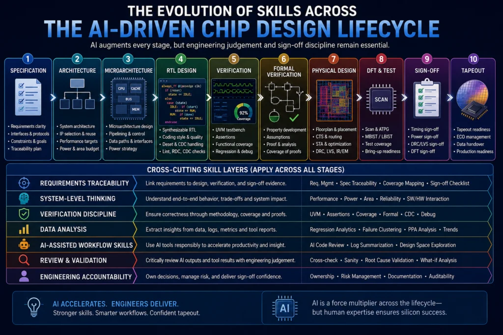
AI adoption does not remove traditional semiconductor engineering skills. Instead, it adds a new layer of workflow, data and review capabilities across the entire design lifecycle. As shown in Figure 2, successful AI-driven chip development still begins with strong requirements definition and architecture planning. AI can assist design exploration, implementation optimisation and verification analytics, but engineering judgement remains essential at every stage.
The most effective semiconductor organisations combine traditional design expertise with AI-assisted workflow capabilities, evidence-based review processes and accountable sign-off practices. This is why future engineering leaders will need both deep technical knowledge and the ability to supervise increasingly automated design environments.
What Different Engineering Roles Should Prioritise
AI-driven chip design does not require every engineer to learn the same skills. The learning path should reflect the role.
RTL Engineers
RTL engineers should prioritise specification interpretation, synthesizable design, interface behaviour, reset and clocking discipline, AI-assisted code review, scripting and collaboration with verification teams. Their main AI skill is not prompt writing. It is the ability to review AI-assisted outputs through the lens of hardware behaviour.
Verification Engineers
Verification engineers should prioritise UVM, assertions, functional coverage, regression analysis, log clustering, formal awareness, failure triage and evidence validation. AI-assisted verification has strong potential, but only when it strengthens rather than weakens review quality. SystemVerilog and UVM remain important foundations because they support structured verification, reusable components, coverage and assertion-based methods [6], [7].
Physical Design Engineers
Physical design engineers should prioritise PPA interpretation, constraints, STA, floorplanning, routing awareness, IR drop, electromigration, DRC/LVS, ECO review and design-space optimisation. AI-assisted physical design can accelerate exploration, but engineers must still evaluate whether the result is physically robust and sign-off ready [1], [2], [3].
DFT and Test Engineers
DFT engineers should prioritise scan strategy, ATPG, MBIST, LBIST, boundary scan, coverage analysis, post-silicon debug visibility and test-data interpretation. AI may help analyse failure patterns, but test strategy still requires design and manufacturing context. This becomes increasingly important as manufacturing environments use AI and analytics for yield optimisation, predictive maintenance and defect monitoring [8], [9].
Engineering Managers and Technical Leads
Technical leads should prioritise workflow integration, governance, pilot measurement, secure deployment, team training and sign-off accountability. Their role is to ensure AI adoption improves engineering throughput without creating uncontrolled risk.
What Teams Often Get Wrong About AI-Driven Chip Design
The most common mistake is treating AI-driven chip design as a tool purchase rather than a workflow transformation. A tool that is not connected to specifications, verification plans, regression systems, implementation flows, issue tracking and sign-off evidence will usually have limited impact.
The second mistake is overtrust. AI outputs can be useful, but they need to be reviewed as engineering evidence. A fluent explanation does not prove design correctness. A plausible code suggestion does not prove synthesis safety. A coverage recommendation does not prove verification completeness.
The third mistake is weak data discipline. AI-assisted workflows depend on accessible, accurate and well-structured engineering data. If specifications are fragmented, logs are inconsistent, coverage reports are not reviewed properly and issue trackers are incomplete, AI output quality will suffer.
The fourth mistake is ignoring security. Semiconductor design involves confidential IP, customer data, tool scripts, internal architecture documents and sensitive programme information. Organisations need clear rules for what data can be used, where prompts are stored, who can access outputs and how AI-assisted decisions are reviewed.
These issues are why choosing an AI in DV partner should involve methodology, governance, workflow integration and review accountability, not only AI tool features.
How Teams Should Build AI-Driven Chip Design Capability
Engineering teams should build AI-driven chip design capability gradually and measurably.
The best starting point is usually a controlled pilot connected to a known engineering pain point. This could be regression triage, log summarisation, coverage review, documentation retrieval, PPA reporting or implementation-flow analysis. A useful pilot should define the workflow, baseline metrics, expected improvement, review process, security boundary and ownership model. For example, if the goal is regression triage improvement, teams should measure debug preparation time, failure clustering accuracy, duplicate reduction, engineer review time and bug handoff quality.
AI adoption should also be supported by structured training. Engineers need to understand how AI fits into their actual workflows, not only how the tools operate. Alpinum’s engineering training services are relevant where teams need to build capability across verification, methodology and workflow maturity. Larger teams may need role-specific upskilling. RTL engineers, verification engineers, physical design engineers, DFT engineers and technical managers need different levels of AI literacy. For distributed engineering groups, token-based training for engineering teams may provide a practical way to support different learning needs without forcing every engineer through the same path.
The central principle is simple: AI-driven chip design capability should be measured by engineering outcomes, not by the number of tools deployed. Tool capability matters, but outcomes such as improved design exploration, better verification visibility, stronger implementation review and controlled sign-off are what determine engineering value [1], [3], [4].
What Will Matter Most After 2026
After 2026, the most valuable semiconductor engineers will be those who can combine domain expertise with AI-assisted workflow literacy. This means engineers who understand architecture intent, RTL behaviour, verification evidence, implementation constraints, sign-off requirements and data-driven workflow improvement. It also means engineers who can critically review AI outputs rather than accept them simply because they appear confident.
AI may reduce some repetitive engineering effort, but it will increase the value of engineers who can supervise complex workflows, interpret evidence, manage trade-offs and maintain accountability. The future skill set is therefore not AI but engineering. It is stronger engineering supported by better automation, better data use and better workflow integration.
That is the real opportunity in AI-driven chip design from spec to tapeout.
Conclusion
AI-driven chip design changes the skills engineers need, but it does not remove the need for engineering judgement. From specification to tapeout, semiconductor teams still need architecture clarity, RTL discipline, verification methodology, formal reasoning, physical implementation awareness, DFT knowledge, sign-off evidence and accountable review.
AI can support design exploration, workflow automation, regression triage, documentation retrieval and optimisation. However, the value comes from integrating AI into real engineering workflows with traceability, governance and review discipline. The strongest teams will not simply use AI tools. They will build AI-capable engineering processes.
For semiconductor organisations, the practical objective is clear: develop engineers who can use AI to improve design productivity without weakening specification quality, verification confidence or tapeout readiness.
Build AI-Driven Chip Design Capability Without Weakening Sign-Off Confidence
AI can improve productivity across specification review, RTL, verification, implementation and tapeout preparation, but only when it is integrated into accountable engineering workflows.
Alpinum Consulting helps semiconductor teams strengthen verification methodology, workflow maturity, training and safe AI-assisted engineering adoption.
Explore AI in DV Adoption
Discuss Your Verification Workflow
References
[1] Synopsys, “AI chip design: AI-powered EDA solutions,” Synopsys. [Online]. Available: https://www.synopsys.com/ai/ai-powered-eda.html
[2] Synopsys, “DSO.ai: AI-driven design applications,” Synopsys. [Online]. Available: https://www.synopsys.com/ai/ai-powered-eda/dso-ai.html
[3] Cadence Design Systems, “Cadence Cerebrus AI Studio,” Cadence. [Online]. Available: https://www.cadence.com/en_US/home/tools/digital-design-and-signoff/soc-implementation-and-floorplanning/cadence-cerebrus-ai-studio.html
[4] Synopsys, “What is AI-driven chip design?” Synopsys. [Online]. Available: https://www.synopsys.com/glossary/what-is-ai-driven-chip-design.html
[5] Cadence Design Systems, “Cerebrus Intelligent Chip Explorer,” Cadence. [Online]. Available: https://www.cadence.com/en_US/home/tools/digital-design-and-signoff/soc-implementation-and-floorplanning/cerebrus-intelligent-chip-explorer.html
[6] IEEE Standards Association, “IEEE 1800-2023: IEEE standard for SystemVerilog unified hardware design, specification, and verification language,” IEEE. [Online]. Available: https://standards.ieee.org/ieee/1800/7743/
[7] Accellera Systems Initiative, “Universal Verification Methodology,” Accellera. [Online]. Available: https://www.accellera.org/downloads/standards/uvm
[8] SEMI, “Edge AI in semiconductor manufacturing: Powering smart, resilient fabs,” SEMI. [Online]. Available: https://www.semi.org/en/blogs/edge-ai-in-semiconductor-manufacturing-powering-smart-resilient-fabs
[9] SEMI, “AI techniques in semiconductor manufacturing,” SEMI. [Online]. Available: https://www.semi.org/en/event/ai-techniques-workshop
FAQ
The most important skills include requirements traceability, architecture judgement, RTL review, verification methodology, formal reasoning, physical implementation awareness, DFT understanding, sign-off discipline and AI output validation.
AI can support design-space exploration, PPA optimisation, constraint tuning, reporting and implementation-flow analysis. Engineers still need to review timing, power, area, routing, DRC, LVS and sign-off evidence [1], [2], [3].
AI can support comparison, documentation retrieval, and design exploration, but architectural decisions still require engineering judgement regarding performance, power, latency, protocols, integration risk, and verification complexity [1], [4].
AI can help analyse regressions, summarise logs, cluster failures and highlight coverage gaps. It should not replace verification planning, functional coverage intent, assertion review or accountable sign-off decisions [6], [7].
Formal verification strengthens the quality of evidence by proving properties defined under stated assumptions. AI may help with workflow support or property search, but formal confidence still depends on property quality and engineering review [6], [7].
No. AI tools can support parts of the design and implementation flow, but tapeout still requires specification review, verification closure, timing sign-off, physical verification, DFT readiness, ECO control and accountable engineering approval.
Teams should review AI-generated outputs against architecture intent, protocol correctness, reset and clocking behaviour, synthesis suitability, timing impact, verification coverage and sign-off risk.
Because tapeout decisions must be reproducible, traceable and accountable. AI can support analysis, but final sign-off depends on verified evidence, engineering ownership and controlled release processes.

Written by : Mike Bartley
Mike started in software testing in 1988 after completing a PhD in Math, moving to semiconductor Design Verification (DV) in 1994, verifying designs (on Silicon and FPGA) going into commercial and safety-related sectors such as mobile phones, automotive, comms, cloud/data servers, and Artificial Intelligence. Mike built and managed state-of-the-art DV teams inside several companies, specialising in CPU verification.
Mike founded and grew a DV services company to 450+ engineers globally, successfully delivering services and solutions to over 50+ clients.
Mike started Alpinum in April 2016 to deliver a range of start-of-the art industry solutions:
Alpinum AI provides tools and automations using Artificial Intelligence to help companies reduce development costs (by up to 90%!) Alpinum Services provides RTL to GDS VLSI services from nearshore and offshore centres in Vietnam, India, Egypt, Eastern Europe, Mexico and Costa Rica. Alpinum Consulting also provides strategic board level consultancy services, helping companies to grow. Alpinum training department provides self-paced, fully online training in System Verilog, UVM Introduction and Advanced, Formal Verification, DV methodologies for SV, UVM, VHDL and OSVVM and CPU/RISC-V. Alpinum Events organises a number of free-to-attend industry events
You can contact Mike (mike@alpinumconsulting.com or +44 7796 307958) or book a meeting with Mike using Calendly (https://calendly.com/mike-alpinum-consulting).
Stay Informed and Stay Ahead
Latest Articles, Guides and News
Explore related insights from Alpinum that dive deeper into design verification challenges, practical solutions, and expert perspectives from across the global engineering landscape.