
AI Demand Is Growing Faster Than Manufacturing Capacity
Artificial intelligence is transforming the semiconductor industry at a pace rarely seen before. Every major technology company is investing in larger AI models, cloud infrastructure, autonomous systems and edge computing, all of which require increasingly sophisticated semiconductor devices.
Against this backdrop, Taiwan Semiconductor Manufacturing Company (TSMC) has announced one of the largest manufacturing investments in semiconductor history. Recent announcements indicate that the company plans to invest approximately US$265 billion in expanding manufacturing capacity in the United States, including multiple fabrication plants, advanced packaging facilities and research capabilities focused on future semiconductor technologies.
For most readers, the headline is about manufacturing.
For semiconductor engineers, however, another question deserves equal attention.
Can verification capacity grow quickly enough to support the next generation of AI chips?
Manufacturing capacity alone cannot deliver competitive AI processors. Every advanced device entering a fabrication facility must first complete an increasingly demanding verification programme capable of proving functional correctness, safety, security and performance across billions of transistors.
This growing verification challenge is likely to become one of the industry’s biggest bottlenecks over the coming decade. For organisations developing AI accelerators, CPUs, GPUs and custom ASICs, engineering capability may become just as important as manufacturing capability.
Learn how modern verification teams are adapting through our AI in Design Verification services and frameworks.
Why TSMC’s US Expansion Matters
The latest expansion significantly increases TSMC’s long-term commitment to manufacturing in Arizona.
The investment supports several strategic objectives:
- Increasing US semiconductor production
- Reducing supply-chain risk
- Supporting national security initiatives
- Expanding advanced packaging
- Producing future 2 nm technologies
- Meeting rapidly increasing AI demand
This investment is not simply about producing more chips.
It represents an attempt to support the next generation of AI infrastructure expected to power:
- Hyperscale data centres
- Generative AI
- Autonomous vehicles
- Robotics
- Medical AI
- Industrial automation
- Defence electronics
- Edge AI systems
Demand continues to accelerate because every new AI model requires significantly more compute capability than previous generations. At the same time, customers expect shorter development cycles. This places unprecedented pressure on semiconductor engineering teams.
Manufacturing Is Only One Part of the Challenge
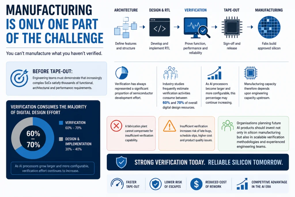
Advanced fabs cannot manufacture devices that have not completed verification.
Before tape-out, engineering teams must demonstrate that increasingly complex System-on-Chips satisfy thousands of functional, architectural and performance requirements. Verification has always represented a significant proportion of semiconductor development effort. Industry studies frequently estimate verification activities consume between 60% and 70% of overall digital design resources.
As AI processors become larger and more configurable, this percentage may continue increasing. Manufacturing capacity therefore depends upon engineering capacity upstream. A fabrication plant cannot compensate for insufficient verification capability. Organisations planning future AI products should therefore invest not only in silicon manufacturing but also in scalable verification methodologies and experienced engineering teams.
Discover how Design Verification Services support complex SoC development programmes.
AI Chips Are Becoming Exceptionally Complex
The semiconductor devices entering production today differ dramatically from processors manufactured only five years ago.
Modern AI accelerators integrate:
- Massive parallel processing
- High-bandwidth memory interfaces
- Advanced cache hierarchies
- Chiplets
- Complex interconnects
- Dedicated AI engines
- Security processors
- Heterogeneous compute architectures
Each additional subsystem increases verification complexity. Rather than verifying isolated RTL blocks, engineering teams increasingly verify complete computing platforms. Every interface introduces additional scenarios requiring coverage. Every configurable feature expands the state space. Every software interaction creates new corner cases. As a result, verification schedules grow faster than RTL implementation.
2 nm Technology Raises the Verification Standard
TSMC’s roadmap includes manufacturing technologies centred on 2 nm production. Although process technology primarily affects manufacturing, it indirectly increases verification complexity.
Smaller geometries enable:
- Larger SoCs
- Additional AI accelerators
- More processor clusters
- Greater cache capacity
- Higher integration
- Improved performance per watt
Design teams naturally use these capabilities to build more sophisticated products. Consequently, verification environments must also evolve.
Larger designs require:
- Improved simulation performance
- Scalable regression infrastructure
- Better coverage management
- Stronger formal verification
- Intelligent debug automation
Simply adding more simulations is unlikely to remain economically sustainable. Engineering teams increasingly require automation capable of identifying high-risk verification gaps earlier.
Read more about how AI is changing semiconductor engineering.
Verification Capacity May Become the Real Bottleneck
The semiconductor industry often discusses fabrication capacity. Far less attention is given to verification capacity. Unlike manufacturing equipment, verification expertise cannot be purchased quickly.
Experienced verification engineers require years of practical project experience across:
- SystemVerilog
- UVM
- Formal verification
- Assertion-based verification
- Emulation
- FPGA prototyping
- Coverage closure
- Debugging
Demand for these specialists continues increasing across AI, automotive, aerospace, networking and data-centre markets. If manufacturing expands faster than engineering capability, verification schedules may become the limiting factor for product delivery.
This is particularly relevant for organisations pursuing aggressive AI roadmaps. Every delayed tape-out postpones manufacturing. Every verification escape increases downstream cost. Every late bug threatens programme schedules. Consequently, verification capacity deserves strategic attention alongside wafer capacity.
Advanced Packaging Creates New Verification Challenges

The expansion also includes advanced packaging technologies, particularly CoWoS, which have become essential for AI accelerators.
Modern AI systems increasingly combine:
- GPUs
- Chiplets
- HBM memory
- High-speed interconnects
Although packaging occurs after silicon production, engineering teams must verify interactions much earlier. Verification increasingly extends beyond individual RTL blocks into complete heterogeneous systems. This requires broader expertise covering architecture, software interaction, performance analysis and hardware integration.
AI Is Also Transforming Verification
Ironically, AI may help solve part of the verification challenge.
Engineering teams increasingly evaluate AI-assisted approaches for:
- Regression analysis
- Coverage prioritisation
- Assertion generation
- Log analysis
- Bug classification
- Test generation
- Root-cause investigation
AI does not replace engineering judgement. Instead, it allows verification specialists to spend more time solving complex design problems rather than repetitive manual tasks.
Explore how AI in Design Verification supports practical engineering adoption.
What This Means for Semiconductor Companies
TSMC’s manufacturing expansion signals confidence in long-term AI demand. However, successful semiconductor programmes will depend upon more than fabrication investment.
Leading organisations should strengthen:
- Verification methodologies
- Engineering capability
- AI-assisted workflows
- Reusable verification IP
- Formal verification
- Continuous integration
- Functional coverage strategies
- Workforce development
Companies that invest early in scalable verification capability are likely to reach tape-out faster while reducing technical risk.
Conclusion
TSMC’s US$265 billion expansion represents one of the most significant manufacturing investments in semiconductor history and reflects the industry’s confidence in sustained AI demand.
Yet the real challenge extends beyond constructing fabs. Every advanced AI processor must first pass through an increasingly complex verification process that determines whether a design is ready for silicon. As AI accelerators integrate more compute, memory, chiplets and advanced packaging technologies, verification capacity is becoming a strategic resource in its own right. Organisations that combine manufacturing access with strong verification expertise, automation and skilled engineering teams will be better positioned to deliver reliable products on schedule.
For semiconductor companies planning future AI programmes, investing in verification capability today may prove just as important as investing in manufacturing capacity tomorrow.
IEEE References
[1] TSMC, Annual Report and Investor Information. Available: https://investor.tsmc.com/
[2] Associated Press, “TSMC expands U.S. investment for advanced semiconductor manufacturing.”
[3] Semiconductor Industry Association, State of the U.S. Semiconductor Industry.
[4] Semiconductor Engineering, “Verification Complexity in Advanced SoCs.”
[5] Accellera Systems Initiative, Universal Verification Methodology (UVM) Standard.
FAQs
The investment supports advanced semiconductor manufacturing, AI chip demand, supply-chain resilience and future 2 nm production.
AI processors contain billions of transistors, heterogeneous architectures, high-bandwidth memory, chiplets and increasingly complex software interactions, all of which expand the verification workload.
AI can improve productivity by assisting with test generation, coverage analysis, log review and debug, but experienced verification engineers remain essential for validating complex semiconductor designs.
Greater manufacturing capacity creates opportunities for AI chip development, but companies must also invest in verification capability, engineering skills and scalable design methodologies to deliver products successfully.

Written by : Mike Bartley
Mike started in software testing in 1988 after completing a PhD in Math, moving to semiconductor Design Verification (DV) in 1994, verifying designs (on Silicon and FPGA) going into commercial and safety-related sectors such as mobile phones, automotive, comms, cloud/data servers, and Artificial Intelligence. Mike built and managed state-of-the-art DV teams inside several companies, specialising in CPU verification.
Mike founded and grew a DV services company to 450+ engineers globally, successfully delivering services and solutions to over 50+ clients.
Mike started Alpinum in April 2016 to deliver a range of start-of-the art industry solutions:
Alpinum AI provides tools and automations using Artificial Intelligence to help companies reduce development costs (by up to 90%!) Alpinum Services provides RTL to GDS VLSI services from nearshore and offshore centres in Vietnam, India, Egypt, Eastern Europe, Mexico and Costa Rica. Alpinum Consulting also provides strategic board level consultancy services, helping companies to grow. Alpinum training department provides self-paced, fully online training in System Verilog, UVM Introduction and Advanced, Formal Verification, DV methodologies for SV, UVM, VHDL and OSVVM and CPU/RISC-V. Alpinum Events organises a number of free-to-attend industry events
You can contact Mike (mike@alpinumconsulting.com or +44 7796 307958) or book a meeting with Mike using Calendly (https://calendly.com/mike-alpinum-consulting).
Stay Informed and Stay Ahead
Latest Articles, Guides and News
Explore related insights from Alpinum that dive deeper into design verification challenges, practical solutions, and expert perspectives from across the global engineering landscape.