
The semiconductor industry outlook for 2026 is defined by two realities. Demand for artificial intelligence computing is accelerating investment in processors, memory, advanced packaging and manufacturing capacity. At the same time, the engineering effort required to design, integrate and verify those systems is rising sharply.
AI accelerators are becoming more specialised. High Bandwidth Memory is becoming central to system performance. Chiplets are changing the boundaries between architecture, packaging and manufacturing. Automotive, industrial and edge platforms are integrating more local intelligence. Across all these markets, verification is becoming a decisive programme constraint.
The companies most likely to succeed will not simply be those able to place more transistors on silicon. They will be those able to convert architectural ambition into reliable products through disciplined design, system-level verification, software integration and controlled use of AI-assisted engineering.
Five Key Learning Points
| Key learning point | Why it matters |
| AI is the strongest growth driver in the semiconductor industry in 2026. | Data-centre training, inference, edge AI and custom silicon are increasing demand for advanced logic, memory, networking and packaging. |
| Memory bandwidth is becoming as important as processor throughput. | AI processors cannot sustain useful performance unless data can move rapidly and efficiently between memory and compute resources. |
| Chiplets and advanced packaging are changing system architecture. | Performance, power, manufacturing yield and verification must increasingly be considered across multiple dies and the complete package. |
| Verification complexity is growing faster than individual design complexity. | Heterogeneous compute, software, security, safety and third-party IP create interactions that cannot be addressed by isolated block-level testing alone. |
| AI can improve verification productivity, but engineering control remains essential. | Generated testbenches, coverage recommendations and failure classification must remain traceable, reproducible and subject to human review. |
The Semiconductor Market in 2026
The semiconductor market has entered an unusually strong but highly concentrated growth cycle.
The latest World Semiconductor Trade Statistics forecast projects global semiconductor sales of more than US$1.5 trillion in 2026, with memory and logic leading the expansion. The Semiconductor Industry Association attributes much of this growth to AI infrastructure and the associated requirement for high-value processors and memory.
Headline growth should nevertheless be interpreted carefully. The industry is not expanding uniformly.
AI accelerators, leading-edge logic, networking silicon and advanced memory are experiencing intense demand. Other segments remain more closely tied to replacement cycles, industrial investment, automotive production or consumer spending. This creates a market in which overall revenue can grow rapidly while individual product categories, manufacturing nodes and regional supply chains experience very different conditions.
The 2026 outlook is therefore best understood as a reallocation of semiconductor value.
More value is moving towards:
- AI compute
- High Bandwidth Memory
- advanced packaging
- custom accelerators
- high-speed interconnect
- data-centre networking
- power delivery and thermal management
- verification and system integration
Deloitte’s 2026 industry outlook estimates that chips supporting generative AI could approach US$500 billion in annual revenue. Although forecasts remain sensitive to infrastructure spending and AI adoption, the scale of the estimate illustrates how strongly AI has changed semiconductor investment priorities.
For engineering organisations, the significance extends beyond market size. AI demand is influencing which products are developed, which process technologies receive investment and where engineering bottlenecks appear.
Why AI Chips Are Reshaping the Semiconductor Industry
Artificial intelligence workloads differ from conventional computing workloads in several important ways.
Training a large model involves repeated parallel mathematical operations across enormous datasets. Inference requires models to produce useful responses quickly, often for many users or devices simultaneously. Both depend on high computational throughput, rapid memory access and efficient movement of data across the system.
A general-purpose CPU remains essential for control, orchestration and software execution. However, it is rarely the most efficient device for every AI calculation. Modern AI platforms therefore combine several types of processing resource.
| Processing architecture | Primary strength | Common role in AI systems |
| CPU | Flexibility and general-purpose control | Operating systems, orchestration and serial workloads |
| GPU | Highly parallel computation | Model training and large-scale inference |
| Custom ASIC | Workload-specific efficiency | Data-centre acceleration and high-volume inference |
| NPU | Efficient neural-network processing | Mobile, automotive and edge AI |
| FPGA | Reconfigurability and low-latency processing | Prototyping, acceleration and evolving algorithms |
| DSP | Efficient signal processing | Audio, imaging, communications and sensor processing |
This diversity is driving heterogeneous system architectures in which different workloads are assigned to the processing element best suited to execute them.
It also explains the growth of custom silicon.
Cloud providers and large technology companies are increasingly evaluating or developing processors designed around their own models, data flows, software environments and operating costs. Custom AI inference silicon can reduce dependence on a single merchant processor architecture and can improve performance per watt for predictable workloads.
However, customisation transfers more engineering responsibility to the organisation developing the device. Architecture, RTL, memory control, software, security, packaging and verification all become part of the programme risk.
Teams considering specialised accelerators therefore need to evaluate not only expected peak performance, but also:
- workload stability
- software ecosystem maturity
- memory behaviour
- data movement
- utilisation
- power delivery
- verification effort
- manufacturing volume
- long-term programmability
Where requirements remain fluid, FPGA design and acceleration services can support architecture exploration, prototyping and low-latency acceleration before a fixed custom-silicon implementation is justified.
Training Versus Inference: Different Silicon Priorities
The distinction between AI training and inference is increasingly important.
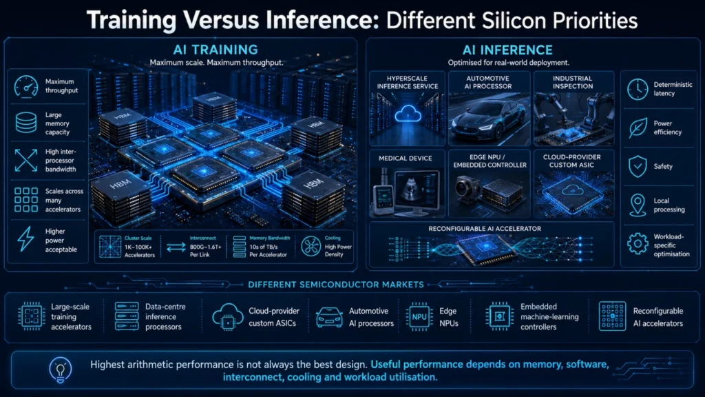
Training platforms generally prioritise maximum throughput, large memory capacity, high inter-processor bandwidth and the ability to scale across many accelerators. These systems can accept substantial power consumption where the computational output justifies the infrastructure cost.
Inference requirements are more diverse.
A hyperscale inference service may still require extensive accelerator clusters. An automotive perception processor, an industrial inspection system, or a medical device may instead prioritise deterministic latency, power efficiency, safety, and local processing.
This creates several semiconductor markets under the broad AI label:
- large-scale training accelerators
- data-centre inference processors
- cloud-provider custom ASICs
- automotive AI processors
- edge NPUs
- embedded machine-learning controllers
- reconfigurable AI accelerators
The design with the highest arithmetic performance is not automatically the best solution. Useful performance depends on the complete system, including memory, software, interconnect, cooling and workload utilisation.
The Memory Wall Moves to the Centre of AI Chip Design
AI systems require enormous quantities of data to move between memory and processing resources. As compute performance increases, memory bandwidth and memory capacity can prevent processors from reaching their theoretical throughput.
This is commonly described as the memory wall.
The challenge is not simply storing a large model. The system must supply model parameters and intermediate data at sufficient speed, with acceptable latency and energy consumption.
For many AI workloads, moving data can consume more energy than performing the arithmetic itself. This means memory architecture affects:
- application performance
- accelerator utilisation
- package design
- power consumption
- thermal behaviour
- system cost
- verification scope
Memory has therefore moved from a supporting component to a defining architectural resource.
Why High Bandwidth Memory Matters in 2026
High Bandwidth Memory uses vertically stacked DRAM dies positioned close to the processor. Through-Silicon Vias and wide interfaces allow large quantities of data to move between memory and compute resources more efficiently than would normally be possible using conventional off-package memory connections.
HBM is particularly valuable for AI acceleration because it provides:
- high aggregate bandwidth
- strong bandwidth density
- shorter interconnect distances
- improved energy efficiency per transferred bit
- large memory capacity within the processor package
The transition towards HBM4 increases the importance of co-design between memory, logic, packaging and the memory-controller architecture.
For verification teams, this creates challenges that extend beyond proving that a controller follows a protocol. Engineers must consider traffic behaviour, ordering, error handling, reset, power management, thermal conditions and interactions between the memory system and multiple compute engines.
| Memory technology | Main advantage | Typical application | Principal engineering challenge |
| HBM | Extremely high bandwidth close to compute | AI accelerators and high-performance computing | Package complexity, thermal behaviour and controller verification |
| DDR5 | Capacity and established server ecosystem | Servers, workstations and infrastructure | Signal integrity, training and high-speed interface validation |
| LPDDR | Reduced power consumption | Mobile and edge systems | Low-power state transitions and power-management verification |
| GDDR | High bandwidth at lower integration complexity than HBM | Graphics and selected inference systems | Board routing, power and thermal management |
| CXL-attached memory | Flexible memory expansion and pooling | Data centres and composable infrastructure | Coherency, latency, interoperability and system software |
The correct memory technology depends on workload, volume, cost and packaging constraints. HBM is not automatically appropriate for every AI processor. Edge and embedded systems may achieve better results using LPDDR or other memory arrangements if power and cost matter more than absolute bandwidth.
Chiplets Move from Option to Architectural Strategy
Large monolithic dies become increasingly expensive and difficult to manufacture as advanced process technology becomes more complex. A single defect can affect the yield of an entire die, while not every function benefits equally from the newest process node.
Chiplets offer another approach.
A chiplet-based system divides functionality across multiple dies integrated within one package. Compute logic can use an advanced process, while analogue interfaces, I/O, security, cache or power-management functions can use technologies better suited to their requirements.
A chiplet system may combine:
- CPU dies
- GPU or accelerator dies
- cache dies
- I/O dies
- memory-controller dies
- security functions
- analogue interfaces
- HBM stacks
This provides several potential benefits.
Smaller dies can improve manufacturing yield. Proven components may be reused across multiple products. Different functions can be manufactured using different process technologies. Product families can be created by changing the number or combination of chiplets.
The architectural boundary, however, has not disappeared. It has moved.
Functions that previously communicated through on-die interconnect must now communicate across physical die-to-die interfaces. Latency, bandwidth, clocking, power states, error behaviour and package reliability all become part of system design.
The UCIe Consortium is developing an open chiplet ecosystem for on-package interconnection. Its current UCIe 3.0 specification extends the standard to higher data rates and enhanced manageability, illustrating how rapidly die-to-die connectivity is becoming part of mainstream system architecture.
Why Chiplets Make Verification More Difficult
A chiplet architecture creates several layers of verification.
Each die must be verified individually. Die-to-die interfaces must be verified for protocol correctness and error recovery. The integrated package must then be assessed as a complete system.
This creates questions such as:
- Does each chiplet conform to its interface contract?
- Can independent reset or power events create invalid system states?
- What happens when a link is degraded or temporarily unavailable?
- Are cache-coherency rules preserved across chiplet boundaries?
- Can errors propagate from one die into another subsystem?
- Can debug data identify the originating chiplet?
- Are security and privilege boundaries preserved across the package?
- Does firmware initialise every combination correctly?
These issues are difficult because chiplets may be designed by different teams or companies. Models may arrive at different abstraction levels. Individual components may have independent release schedules, assumptions and verification environments.
System-level verification must therefore begin before all physical chiplets are available. Architectural models, interface assertions, emulation, virtual platforms and reusable verification components become critical.
The industry is also developing package-level debug mechanisms. MIPI’s Debug over UCIe work reflects the need to observe and diagnose systems containing multiple chiplets without relying solely on external package access.
Advanced Packaging Becomes Part of System Design
Packaging can no longer be treated as a manufacturing activity considered only after logical design has been completed.
In AI and high-performance systems, package architecture influences:
- memory bandwidth
- die-to-die latency
- power delivery
- signal integrity
- cooling
- mechanical reliability
- manufacturing yield
- testability
Technologies such as silicon interposers, 2.5D integration, 3D stacking, fan-out packaging and hybrid bonding allow more compute and memory to be placed within a tightly integrated system.
The package is effectively becoming part of the computer architecture.
This requires closer collaboration between digital designers, analogue engineers, package specialists, power engineers, thermal specialists and verification teams.
The analogue and physical behaviour of high-speed interfaces also becomes more important. Organisations integrating digital processing, high-speed I/O, sensors, power management or analogue interfaces need verification strategies that extend beyond pure RTL simulation. Alpinum’s analogue and mixed-signal design and verification services address this wider interaction between digital logic and real electrical behaviour.
Foundry and Manufacturing Investment Remains AI-Led
AI demand is influencing capital investment across foundries, memory manufacturing and advanced packaging.
SEMI expects worldwide 300 mm fab-equipment spending to increase by 18% to US$133 billion in 2026. The organisation identifies AI chips, edge devices and regional semiconductor self-sufficiency as major drivers of expansion.
SEMI also reported that semiconductor manufacturing-equipment sales reached US$135.1 billion in 2025, an increase of 15%, supported by advanced logic, memory and AI-related capacity investment.
These investments indicate confidence in long-term semiconductor demand, but they do not eliminate supply risk.
Leading-edge fabrication, HBM production and advanced packaging require different equipment, materials, expertise and manufacturing capacity. A system may depend on sufficient supply across all three. Additional wafer capacity alone does not resolve a shortage in memory stacks or package integration.
Engineering leaders therefore need to consider supply-chain constraints during architecture definition. A technically optimal component that cannot be sourced reliably may create more programme risk than a slightly less efficient but widely available alternative.
Semiconductor Sovereignty and Regional Capacity
Governments continue supporting domestic or regional semiconductor manufacturing to reduce dependence on geographically concentrated supply chains.
The result is greater investment in fabrication, packaging, research and workforce development across the United States, Europe, Japan, India and other regions.
Regional expansion can improve resilience, but building a fabrication facility is only one part of a semiconductor ecosystem. Sustainable capacity also requires:
- experienced process engineers
- equipment and materials suppliers
- design capability
- packaging and test
- EDA infrastructure
- verification expertise
- skilled software teams
- reliable customer demand
The workforce issue is especially important. More manufacturing and design programmes increase competition for engineers already experienced in SystemVerilog, UVM, formal verification, analogue design, packaging and embedded software.
This makes professional development a strategic activity rather than an optional benefit. Structured semiconductor verification training can help organisations develop internal capability instead of depending entirely on a constrained external labour market.
Automotive Semiconductors: Growth with Higher Assurance Requirements
Automotive semiconductor demand is being driven by electrification, advanced driver-assistance systems, centralised vehicle computing, connectivity and software-defined vehicle architectures.
Modern vehicles may include processors for:
- perception
- sensor fusion
- driver monitoring
- battery management
- motor control
- infotainment
- secure communications
- vehicle networking
- over-the-air software updates
The engineering challenge differs from that of a data-centre accelerator.
Automotive devices must often behave predictably across temperature, voltage, ageing and fault conditions. They may need to remain available for many years and provide evidence supporting safety and security requirements.
An AI inference engine used for perception cannot be verified only by measuring average model accuracy. The surrounding hardware must correctly move sensor data, schedule workloads, isolate memory, handle faults and communicate with safety mechanisms.
This expands the verification problem across hardware, software and system behaviour.
Formal methods are particularly useful where critical properties must hold across large numbers of possible states. Teams developing safety- or security-sensitive products can build capability through formal verification training for hardware and software, covering proof objectives, assertions, constraints and formal evidence.
Edge AI Expands Beyond the Data Centre
Not every AI workload belongs in the cloud.
Processing data locally can reduce latency, limit network traffic, protect sensitive information and allow equipment to operate when connectivity is unavailable.
Edge AI is therefore expanding across:
- industrial inspection
- robotics
- telecommunications
- smart cameras
- medical equipment
- aerospace
- defence
- consumer devices
- predictive maintenance
These products frequently operate under stricter power, thermal and cost constraints than data-centre systems.
An edge AI processor may need to combine CPU control, sensor interfaces, DSP functions, an NPU, security, memory control and real-time software within a small power envelope. The integration challenge can be more important than the performance of any individual block.
FPGA technology remains relevant in this market because it offers deterministic behaviour, hardware-level parallelism and the ability to adapt interfaces or algorithms after deployment. The choice between FPGA, ASIC, GPU and NPU should be based on the workload, latency, production volume, development schedule and expected rate of algorithmic change.
RISC-V Continues to Expand Architectural Choice
RISC-V provides an open instruction-set architecture that can be implemented and extended for different markets.
It is increasingly relevant to embedded control, research, AI accelerators, security processors and custom SoCs. Its openness enables architectural differentiation without requiring each organisation to create an instruction set from the beginning.
This flexibility also creates verification challenges.
Optional extensions, implementation-specific behaviour, privilege rules, interrupts, memory management and custom instructions expand the number of valid configurations. Verification must address both compliance with the architecture and correct integration into the wider SoC.
A processor can execute individual instructions correctly yet still fail at system level because of cache coherency, interrupt ordering, privilege transitions or interaction with custom accelerators.
RISC-V verification therefore benefits from combining:
- architectural compliance testing
- constrained-random instruction generation
- reference-model comparison
- formal verification
- coverage analysis
- hardware-software co-verification
The open nature of the architecture increases opportunity, but it does not reduce the need for rigorous sign-off.
Verification Becomes the Semiconductor Industry’s Critical Bottleneck
The largest challenge within the 2026 semiconductor outlook may not be designing more functionality. It may be proving that all functionality works correctly.
Modern SoCs combine billions of transistors, third-party IP, configurable processors, multiple clock and power domains, complex software and high-speed interfaces. AI devices add unusual traffic patterns, large memory systems and tightly coupled accelerator architectures. Chiplets add die-to-die communication and package-level dependencies.
Each subsystem may be correct in isolation while the complete product still contains integration failures.
Common verification bottlenecks include:
| Bottleneck | Programme impact |
| Incomplete requirements | Missing tests, weak traceability and late changes |
| Poor verification planning | Unclear ownership, duplicated effort and coverage gaps |
| Fragile testbench architecture | Slow adaptation when RTL or configurations change |
| Long regressions | Delayed feedback and inefficient use of compute resources |
| Coverage plateaus | High simulation cost without meaningful closure |
| Difficult failure triage | Engineers spend time classifying rather than resolving defects |
| Third-party IP assumptions | Integration bugs appear late at SoC level |
| Hardware-software gaps | Firmware exposes behaviour not exercised by block-level tests |
| Weak sign-off evidence | Management cannot judge remaining technical risk |
Alpinum’s ASIC and SoC design verification services support verification planning, UVM environments, regression infrastructure, coverage closure, formal methods, debug and system-level validation.
The important principle is that verification must begin with architecture and requirements. Waiting until RTL is substantially complete creates a reactive process in which teams build tests around an implementation rather than proving the original engineering intent.
Why Simulation Alone Is No Longer Enough
Simulation remains central to semiconductor verification. It provides visibility, supports realistic scenarios and integrates naturally with UVM environments.
However, simulation samples behaviour. It cannot exhaustively explore every possible combination in a complex design.
This becomes particularly important for:
- arbitration
- coherency
- security controls
- deadlock
- privilege logic
- low-power transitions
- protocol corner cases
- fault handling
Formal verification can prove whether specified properties hold across all mathematically reachable states within the defined model and constraints. It is therefore valuable for control-intensive logic and behaviours that are difficult to reach through simulation.
The strongest programmes combine methods.
Simulation addresses realistic traffic, software interaction and system scenarios. Formal verification proves critical properties and explores deep corner cases. Emulation and FPGA prototyping enable larger workloads and earlier software development. Post-silicon validation confirms behaviour in physical hardware.
Verification closure should be based on evidence from the complete strategy rather than a single coverage percentage.
AI in Design Verification: Where It Can Deliver Value
Artificial intelligence is entering verification workflows because the volume of engineering data has become difficult to manage manually.
Regression farms produce large numbers of logs, waveforms, failures and coverage results. Specifications and verification plans contain extensive natural-language information. Testbench development includes repeated patterns. Engineers spend significant time classifying failures, identifying duplicates and deciding where to focus next.
AI can assist with:
- specification analysis
- test-plan drafting
- SystemVerilog and UVM generation
- assertion recommendations
- regression failure clustering
- log summarisation
- coverage-gap identification
- test prioritisation
- debug assistance
- documentation
Alpinum’s AI in Design Verification services focus on integrating these capabilities into established UVM, formal and EDA workflows rather than treating AI as a separate engineering process.
The distinction matters.
A generated testbench is not useful simply because it compiles. It must accurately represent the protocol, drive legal and useful stimulus, detect incorrect behaviour and contribute to measurable verification objectives.
Similarly, an AI-generated assertion must reflect an actual requirement. A plausible but incorrect property can create false confidence.
AI Must Strengthen Evidence, Not Weaken It
Verification sign-off depends on traceability and reproducibility.
Engineers need to know:
- which requirement is being verified
- which test or property addresses it
- how failures are classified
- what coverage has been achieved
- what remains unverified
- who reviewed the result
AI outputs must fit within that evidence chain.
This means organisations need governance for generated code, data access, model selection, review and approval. Sensitive RTL and specifications should not be exposed to uncontrolled systems. Prompts, outputs and tool versions may need to be recorded where reproducibility matters.
Alpinum’s guidance on piloting AI in design verification safely explains why organisations should begin with a bounded workflow, baseline current performance and define measurable success criteria before scaling adoption.
A suitable pilot might focus on failure clustering or log summarisation rather than attempting immediate end-to-end automation. These use cases can deliver measurable productivity improvements while keeping verification decisions under direct engineering control.
Organisations planning wider deployment can also use an AI adoption assessment for semiconductor verification to evaluate capability, data, infrastructure, security and governance before selecting tools.
Agentic Verification and the Move Towards Closed Loops
The next stage of AI-assisted verification is moving beyond one-time code generation towards controlled agentic workflows.
An agentic system may:
- read a specification and RTL interface;
- create a verification plan;
- generate a testbench;
- compile and simulate;
- analyse failures;
- correct testbench issues;
- measure coverage;
- propose additional stimulus;
- repeat within defined limits.
This has significant potential, but the system must distinguish between a genuine RTL defect, a testbench error, an incorrect assumption and a tool-flow problem.
AlpinumDV is being developed around this type of spec-to-verification workflow. The AlpinumDV platform focuses on specification understanding, planning, reference models, generation, simulation, self-debug and coverage closure.
The objective should not be uncontrolled autonomy. It should be faster iteration with clear engineering checkpoints.
What Skills Will Semiconductor Engineers Need?
The 2026 semiconductor industry requires broader engineering capability.
Specialisation remains essential, but engineers increasingly need to understand how their work affects adjacent domains.
Important capability areas include:
System-Level Thinking
Engineers must understand interactions between processors, memory, interconnect, software, packaging and power rather than considering individual blocks in isolation.
Verification Methodology
SystemVerilog, UVM, assertions, coverage, formal verification and regression management remain fundamental.
Hardware-Software Co-Verification
Firmware can configure hardware into states that block-level environments never exercise. Earlier software involvement reduces integration risk.
AI Literacy
Engineers do not all need to become machine-learning researchers. They do need to understand where AI outputs can fail, how to measure productivity and how to maintain review and traceability.
Security and Functional Safety
Connected and autonomous products require verification of isolation, secure boot, privilege, fault response and safe behaviour.
Communication
Large semiconductor programmes are distributed across companies, countries and technical disciplines. Clear requirements, interface agreements and review decisions directly affect engineering quality.
Practical environments such as Alpinum’s Online Submission Portal can support controlled verification exercises using selected EDA flows, prepared designs, custom scripts and repeatable results.
Priorities for Semiconductor Engineering Leaders in 2026
Engineering leaders should avoid responding to industry growth by simply adding more tools or more compute capacity. The most effective response is to improve the engineering system.
Begin Verification at Architecture
Define critical behaviours, interfaces, risks and sign-off evidence before implementation accelerates.
Treat Memory and Packaging as Architectural Decisions
Do not optimise compute independently from bandwidth, power, thermal behaviour and package constraints.
Build a Mixed Verification Strategy
Use simulation, formal verification, emulation, FPGA prototyping and post-silicon validation according to risk.
Pilot AI Against a Measured Baseline
Select a bounded use case, record current effort and compare results using quality and productivity metrics.
Protect Engineering Data
Establish clear rules for RTL, specifications, logs and proprietary information before connecting AI services.
Invest in Internal Capability
Training, mentoring and repeatable methodology provide longer-term value than dependence on individual experts.
Review Supply-Chain Assumptions Early
Confirm whether the required foundry node, memory, package technology and test capacity are commercially realistic.
Build Communities of Practice
Technical events help teams compare approaches and learn from wider industry experience. Alpinum supports this exchange through Verification Futures conferences and DVClub events.
Semiconductor Industry Outlook Beyond 2026
Several trends are likely to continue through the remainder of the decade.
AI processors will become more specialised. Inference will grow relative to training as more organisations deploy models into products and business operations. Memory architecture will remain central to performance and cost. Chiplets will allow more modular systems, although interoperability and verification will remain difficult. Packaging and cooling will influence architectural choices earlier.
At the same time, semiconductor design will become more closely connected to software and AI engineering.
Specifications may increasingly drive automated generation of models, assertions and verification environments. Machine learning may steer stimulus towards coverage gaps. AI assistants may classify failures before an engineer opens a waveform. Formal techniques may be applied more widely as generated properties improve.
None of this removes the need for engineering judgement.
Automation can produce more output. Verification must determine whether that output is correct, complete and aligned with intent.
Conclusion
The semiconductor industry outlook for 2026 is exceptionally strong, but its growth is concentrated around demanding technologies.
AI chips require more compute, memory and network bandwidth. HBM brings memory closer to the processor but increases package and controller complexity. Chiplets improve architectural flexibility while creating new interfaces and failure modes. Advanced packaging becomes part of system design. Edge and automotive applications demand local intelligence under strict power, safety and reliability constraints.
These developments make verification a strategic capability.
Successful organisations will connect architecture, requirements, verification, software, packaging and manufacturing from the beginning of a programme. They will use AI to reduce repetitive work and improve decision support, but they will retain traceability, review and human responsibility for sign-off.
The future of semiconductor engineering will not be determined by transistor count alone. It will be determined by how confidently organisations can convert increasing complexity into working, reliable silicon.
Discuss a Semiconductor Verification Programme
Alpinum Consulting supports organisations working across ASIC, SoC, FPGA, AI-assisted verification, formal methods and semiconductor training.
Explore Alpinum’s design verification services, AI in Design Verification and FPGA engineering services, or contact the Alpinum team to discuss a current programme.
FAQs
The semiconductor market is experiencing strong AI-led growth, with memory, advanced logic, AI accelerators, networking and advanced packaging receiving substantial investment. Growth is significant but concentrated, so conditions vary across product categories.
The strongest drivers include generative AI infrastructure, cloud computing, custom AI accelerators, HBM demand, edge AI, automotive electronics, advanced networking and regional manufacturing investment.
AI processors require extremely high memory bandwidth to keep large numbers of compute units supplied with data. HBM provides high bandwidth close to the processor with improved bandwidth density and energy efficiency.
Chiplets allow different functions to be manufactured as smaller dies and combined within one package. This can improve reuse, manufacturing yield and process-node flexibility, but it increases package-level integration and verification requirements.
The central problem is system interaction. Individual blocks may work correctly while failures emerge through software, memory, third-party IP, power states, security controls or die-to-die communication.
AI can automate parts of planning, testbench generation, regression analysis and coverage improvement. It cannot independently own engineering intent, risk decisions or sign-off accountability. Experienced engineers remain essential.
Begin with a bounded use case, such as log summarisation or failure clustering. Measure the existing workflow, define success criteria, protect design data and maintain human review before expanding to more complex tasks.

Written by : Mike Bartley
Mike started in software testing in 1988 after completing a PhD in Math, moving to semiconductor Design Verification (DV) in 1994, verifying designs (on Silicon and FPGA) going into commercial and safety-related sectors such as mobile phones, automotive, comms, cloud/data servers, and Artificial Intelligence. Mike built and managed state-of-the-art DV teams inside several companies, specialising in CPU verification.
Mike founded and grew a DV services company to 450+ engineers globally, successfully delivering services and solutions to over 50+ clients.
Mike started Alpinum in April 2016 to deliver a range of start-of-the art industry solutions:
Alpinum AI provides tools and automations using Artificial Intelligence to help companies reduce development costs (by up to 90%!) Alpinum Services provides RTL to GDS VLSI services from nearshore and offshore centres in Vietnam, India, Egypt, Eastern Europe, Mexico and Costa Rica. Alpinum Consulting also provides strategic board level consultancy services, helping companies to grow. Alpinum training department provides self-paced, fully online training in System Verilog, UVM Introduction and Advanced, Formal Verification, DV methodologies for SV, UVM, VHDL and OSVVM and CPU/RISC-V. Alpinum Events organises a number of free-to-attend industry events
You can contact Mike (mike@alpinumconsulting.com or +44 7796 307958) or book a meeting with Mike using Calendly (https://calendly.com/mike-alpinum-consulting).
Stay Informed and Stay Ahead
Latest Articles, Guides and News
Explore related insights from Alpinum that dive deeper into design verification challenges, practical solutions, and expert perspectives from across the global engineering landscape.