

Semiconductor growth depends on more than new fabs, investment and EDA tools. Every processor, accelerator, chiplet, sensor interface and embedded system also depends on people who can translate requirements into architecture, implement designs, verify behaviour, write low-level software, analyse failures and make responsible sign-off decisions.
That makes the semiconductor skills gap in 2026 a delivery constraint, not only a recruitment issue. The UK Semiconductor Sector Study 2026 identified 705 semiconductor companies and estimated that dedicated companies directly employed approximately 16,350 people in 2025. Most surveyed firms expected growth, but talent availability remained a persistent barrier that could constrain delivery. [1]
The gap is also international. Europe faces retirement pressure and a slow inflow of new graduates, while the United States projects substantial unfilled demand for technicians, engineers and computer scientists. [3], [6] Universities, employers, professional communities and training providers therefore need to develop capability together.
This article explains which capabilities matter, why traditional academic preparation is not sufficient on its own, how practical laboratories and mentoring can improve readiness, how AI changes the skills mix, and how training effectiveness can be measured through engineering evidence rather than attendance.
Key learning points
| Key learning point | Detailed section | Evidence |
| The gap is driven by growth, complexity, retirement and global competition | Why the Semiconductor Skills Gap Is Growing in 2026 | [1], [2], [3], [6] |
| Roles span design, verification, formal, software, manufacturing and systems | Which Roles and Capabilities Are Most Needed? | [2], [7] |
| Academic foundations need realistic projects and tool access | Why Traditional Academic Preparation Is Not Enough | [2], [8] |
| Employers must create structured early-career pathways | How Employers Can Develop Talent and Create Clear Career Paths | [2], [5] |
| Training must be assessed through practical contribution | Training Pathways for Design, Verification, Formal, Software and RISC-V Roles | [5] |
Why the Semiconductor Skills Gap Is Growing in 2026
The skills gap is the mismatch between the capabilities semiconductor programmes need and the experience available in the labour market. It grows when demand expands faster than training, when experienced specialists retire, and when technical complexity raises the level of judgement required from each team.
Demand is broadening across markets
AI infrastructure is a major driver, but semiconductor demand also comes from automotive systems, industrial automation, communications, defence, medical technology, energy systems and edge computing. These markets need different combinations of architecture, digital and analogue design, verification, firmware, security, packaging and validation.
Alpinum’s Semiconductor Industry Outlook 2026 explains how AI chips, memory demand, chiplets and verification bottlenecks are raising the capability required across the engineering lifecycle.
System complexity is increasing
Modern devices combine configurable intellectual property, processors, accelerators, security features, software-controlled power states, high-speed interfaces and mixed hardware-software behaviour. An engineer may own a bounded block, but decisions increasingly depend on system context. Teams need people who can reason about resets, protocols, performance, safety, security, firmware interaction and sign-off evidence.
Retirement creates a knowledge-transfer risk
The 2025 UK Semiconductor Workforce Study estimated a workforce of approximately 27,245 people, with 69% in technical roles. It estimated that 39%, more than 10,000 workers, could retire within 15 years. Only 0.4% had apprenticeships or foundation degrees as their highest qualification. [2]
Retirement removes more than headcount. Senior engineers often carry tacit knowledge about historical design decisions, recurring failure modes, incomplete specifications, tool limitations and the evidence required for sign-off. Organisations lose this judgement when mentoring and documentation are treated as optional activities.
Regions compete for the same experienced people
The European Chips Skills Academy reported that around 30% of Europe’s semiconductor workforce could retire by 2030, while the inflow of graduates was increasing by less than 1% per year. It estimated an annual shortfall of approximately 10,800 skilled professionals across the European value chain. [3]
The Semiconductor Industry Association projects that the US semiconductor workforce will add nearly 115,000 jobs by 2030, with roughly 67,000 at risk of remaining unfilled at current degree-completion rates. [6] Moving experienced people between regions cannot solve a global shortage. The industry needs to expand the total talent pool.
Career visibility remains limited
Many students understand software careers but have little exposure to RTL design, verification, physical implementation, packaging, process engineering or post-silicon validation. Even relevant degree programmes may provide only brief contact with modern EDA workflows. The industry therefore has a visibility problem before it has a recruitment problem. Students cannot choose pathways they have never seen.
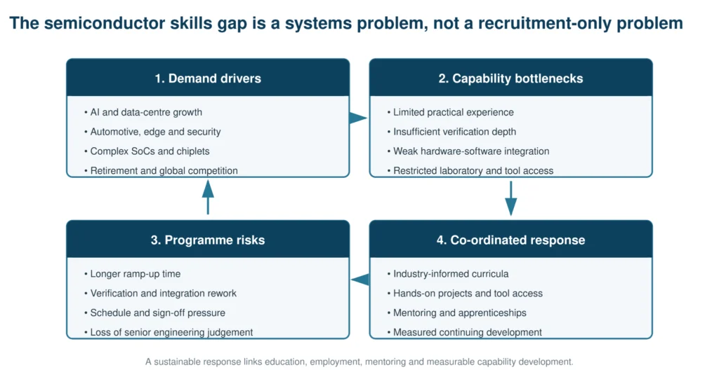
Figure 1: The semiconductor skills gap is created by connected demand, capability and programme factors [1-3].
Which Semiconductor Roles and Capabilities Are Most Needed?
There is no single semiconductor occupation. The industry depends on a connected chain of specialists, and the required mix changes with the product, technology node, business model and stage of development.
The UK workforce study found that design-related work represented 64% of technical roles, with IC design, software development and research particularly prominent. [2] The Council for Science and Technology defines chip designers broadly to include architecture, design, verification, simulation, validation and low-level software. [7]Capability area Core knowledge Evidence of practical readiness Digital design Logic, architecture, RTL, synthesis, clocking, reset, power intent and implementation constraints A synthesised subsystem with reviewed interfaces, lint results and documented decisions Design verification SystemVerilog, UVM, assertions, stimulus, scoreboards, coverage, regressions and debug A verification environment linked to a plan, coverage goals and explained residual risk Formal verification Properties, assumptions, abstraction, proof decomposition, vacuity and convergence Reviewed properties with reproducible results and justified constraints Analogue and mixed-signal Device behaviour, modelling, PVT variation, calibration and cross-domain interaction A model or test environment that demonstrates analogue-digital behaviour Physical implementation Floorplanning, placement, routing, timing, power, signal integrity and closure An implementation flow with analysed timing and power reports Embedded software C, C++, Python or Rust, firmware, drivers, RTOS concepts and hardware bring-up Software that configures, exercises and diagnoses a hardware platform RISC-V and processor engineering ISA behaviour, privilege modes, CSRs, exceptions, interrupts and memory systems Tests or properties that validate processor and SoC behaviour Manufacturing, packaging and test Processes, yield, metrology, chiplets, thermal behaviour, testability and HBM integration Laboratory or production evidence linked to process and package decisions Post-silicon validation Bring-up, instrumentation, diagnostics and correlation with pre-silicon evidence A reproducible validation plan and defect investigation Technical leadership Planning, review, risk, communication, mentoring and cross-functional decisions Evidence of leading a review, resolving a technical issue or improving a workflow
Table 1: Semiconductor roles, knowledge and readiness evidence
Design verification deserves particular attention because it connects requirements, architecture, implementation and sign-off. Organisations requiring delivery support can review Alpinum’s design verification services.
Why Traditional Academic Preparation Is Not Enough
University education remains essential. Semiconductor engineering depends on mathematics, electronics, digital logic, computer architecture, programming, physics and structured problem-solving. The issue is not that academic foundations are unnecessary. The issue is that theory alone does not reproduce the environment of a commercial semiconductor programme.
Nearly half of the semiconductor employers surveyed for the UK workforce study felt that current university courses, particularly undergraduate programmes, did not fully align with industry requirements. [2] Several recurring gaps explain this concern.
Academic exercises are often too well defined
University assignments normally provide a bounded question and expected result. Real specifications may contain ambiguity, conflicting requirements, missing reset behaviour or assumptions that have never been documented. Engineers need practice asking what a requirement means, how it can be observed, which cases are legal and what evidence will demonstrate completion.
Projects may be too small and isolated
A small processor or FPGA exercise can teach useful concepts, but commercial programmes involve many interfaces, contributors and review stages. Students need experience with version control, code review, issue tracking, automated builds, regression results and integration failures. Knowing a language is different from working effectively inside an engineering workflow.
Verification is often introduced too late
Some courses teach students to create a design and then verify it with a few directed tests. That does not prepare them for verification planning, assertions, functional coverage, reusable environments, constrained stimulus, regression management, or systematic debug. Alpinum’s guide to Universal Verification Methodology explains how structured testbenches separate stimulus, observation, prediction, checking and coverage.
Tool access and hardware-software integration are limited
Commercial EDA tools can be expensive and difficult to deploy at scale. Open-source tools improve access, but teaching still needs to explain the engineering purpose behind linting, simulation, synthesis, formal checking and regression analysis. Students also need projects in which firmware interacts with registers, interrupts, memory, peripherals and error conditions.
Judgement develops through practice and feedback
A meta-analysis of 225 undergraduate STEM studies found that active learning improved assessment performance and reduced failure rates compared with traditional lecturing. [8] Semiconductor learning should therefore include decisions, mistakes, reviews and repeated application. Alpinum’s article on learning by doing in semiconductor verification applies this principle directly to engineering training.
How Universities Can Produce More Industry-Ready Engineers
Universities do not need to turn every electronic engineering degree into a narrow vocational programme. They should preserve strong scientific foundations while creating carefully designed opportunities to apply those foundations in realistic semiconductor contexts.
Define observable outcomes with employers
Industry advisory boards should define what graduates should be able to demonstrate, not only which topics a module should mention. Useful outcomes include interpreting a hardware specification, implementing and reviewing a small RTL block, creating a verification plan, analysing coverage, using version control and explaining a technical decision.
Introduce semiconductor contexts early
Students should encounter chip careers before their final year. Early laboratories can connect logic, programming and electronics with real devices. Later modules can add architecture, RTL, verification, firmware and implementation concepts. This staged approach makes the route into the industry visible.
Treat verification as a core discipline
A progressive verification curriculum should cover:
- Requirements analysis
- Verification planning
- Directed and self-checking tests
- Assertions
- Constrained stimulus
- Functional coverage
- Scoreboards and reference models
- Debug and defect reporting
- Regression automation
- Sign-off reasoning
Universities can supplement modules with a structured SystemVerilog and UVM training pathway that includes practical exercises, assertions, coverage, UVM and debug.
Use capstone projects that produce engineering evidence
Capstone projects should generate:
- A requirements document and architecture description
- RTL, software or model repositories
- A verification plan and automated regression scripts
- Test, proof and coverage results
- Known limitations and risk statements
- Code-review and design-review records
- A final technical retrospective
A demonstration on the final day is useful, but the evidence generated throughout the project shows whether students can work in a disciplined and reproducible way.
Create shared access to tools and infrastructure
Not every university can operate a complete advanced semiconductor laboratory. Institutions can share remote EDA environments, cloud-based exercises, containerised open-source flows, FPGA platforms, teaching designs and multi-project wafer access. The UK Council for Science and Technology has recommended a nationally curated chip design course, wider access to design infrastructure and stronger coverage of architecture, design, verification and validation. [7]
Support teaching staff and interdisciplinary work
Short industrial placements, joint projects, guest teaching and access to specialist training can help academic staff connect enduring principles with current engineering workflows. Shared projects can bring together RTL, verification, software, security and implementation teams, giving students experience of interface ownership and integration.
How Employers Can Develop Talent and Create Clear Career Paths
Employers often report that graduates lack industry experience. That experience can only be created when organisations employ and develop people who do not yet have it. Waiting for competitors to train the next generation is not a sustainable strategy.
| Development stage | Main objective | Example activities |
| Foundation | Understand the product, architecture and engineering flow | Product overview, tool setup, coding standards and basic exercises |
| Guided practice | Apply methods in a controlled environment | Small design change, verification component, property set or firmware task |
| Supervised contribution | Work on a real project with review | Bug fix, coverage task, interface verification or software feature |
| Independent ownership | Own a bounded technical area | Plan, implement, review and report a defined responsibility |
| Broader development | Build system awareness and progression | Rotations, architecture reviews, cross-team debug and mentoring |
Table 2: A structured early-career development pathway
Protect learning time
Early-career engineers need real work, but a constant stream of urgent delivery tasks can produce shallow knowledge and repeated mistakes. Protected time for structured exercises, architecture study, historical bug reproduction, pairing and documentation should reduce later supervision and rework.
Create visible technical career paths
Strong engineers should not have to become people managers to progress. Organisations should define parallel routes for individual contributors, methodology specialists, architects, programme leaders, managers, mentors and technical trainers. The UK workforce study recommends clearer technical and managerial progression routes to support retention. [2]
Recruit for foundations and learning potential
Job descriptions should separate essential foundations from skills that can be trained within months and experience that takes years to develop. A candidate with strong logic, architecture and programming foundations may become an effective verification engineer through structured training even without prior commercial UVM experience. Conversion pathways can also open roles to software, physics and mathematics graduates.
Measure development alongside recruitment
Workforce planning should track hiring, mentor capacity, time to useful contribution, retention, internal mobility and succession risk. The aim is not only to fill vacancies. It is to build sustainable capability.
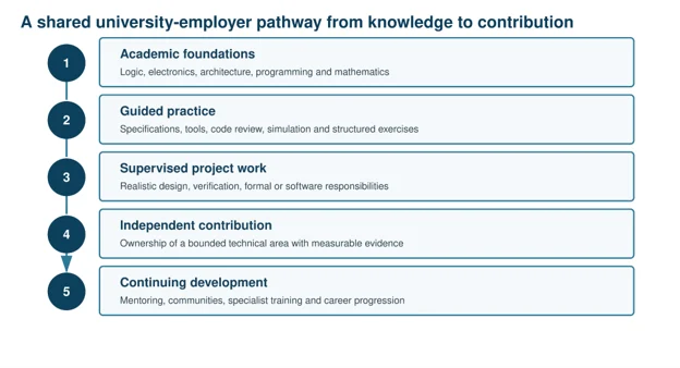
Figure 2: A shared pathway moves engineers from academic foundations to independent contribution and continuing development [4],[5].
The Role of Practical Laboratories, Projects and Tool Access
Practical learning is where abstract knowledge becomes engineering capability. A useful semiconductor laboratory does not need to reproduce a leading-edge fab, but it must let learners make decisions, observe results, investigate failures and explain what the evidence means.
Design exercises around a complete engineering loop
A complete learning loop should require students to:
- Read a short specification
- Identify ambiguity and risk
- Implement or configure a design
- Create a verification or validation plan
- Write tests, checks or properties
- Run an automated flow
- Analyse failures
- Improve coverage or proof quality
- Document limitations
- Present a sign-off recommendation
Use deliberately imperfect designs
Training designs should contain controlled defects such as incorrect reset behaviour, boundary-condition errors, protocol violations, missing assertions, incomplete scoreboards, unsound formal assumptions or firmware sequencing faults. Learners build judgement by discovering, explaining and correcting these issues.
Make environments repeatable and accessible
Remote environments, automation and controlled submissions reduce time lost to inconsistent tool setup. Alpinum’s online self-paced training environment combines lecture material, quizzes, hands-on EDA exercises, automated checking and progress feedback. Alpinum’s online and self-paced training is supported by the Alpinum Online Submission Portal, a controlled environment for running practical verification exercises.
Teach transferable workflow principles
Tools change, but engineering questions remain stable. Learners should understand what simulation demonstrates, what formal analysis proves, how coverage can mislead, why assumptions require review and how traceability supports a decision. A green result is not enough if the learner cannot explain its limits.
Apprenticeships, Mentoring and Knowledge Transfer from Senior Engineers
Apprenticeships can widen entry routes into manufacturing, test, technician, software-support and selected engineering roles. The UK AI Hardware Plan calls for work with employers on pathways into semiconductor and AI hardware careers, including apprenticeships, with particular attention to chip design and verification. [4]
NIST guidance emphasises employer-led programmes, stackable credentials, registered apprenticeships and strategic partnerships that connect training with real jobs. [5] An effective apprenticeship needs a defined target role, paid learning, qualified supervision, progressive responsibility and recognised competencies.
Make mentoring a planned responsibility
A structured mentoring approach should:
- Define mentor and learner expectations
- Protect regular meeting and pairing time
- Use real reviews and debug sessions
- Track evidence of progression
- Recognise mentoring in workload and performance planning
- Provide an escalation route when support is insufficient
Mentoring should not depend on whether a senior engineer happens to have spare time. It must form part of delivery planning because it protects future delivery capability.
Transfer judgement through shared engineering work
Pairing during debug, specification reviews, assertion reviews, architecture walkthroughs, post-project retrospectives and sign-off observation reveals how experienced engineers frame a problem, challenge assumptions and decide whether evidence is sufficient.
Capture knowledge without creating document overload
Concise decision records, failure-mode catalogues, review checklists, example properties, debug playbooks and project retrospectives are often more valuable than long process manuals. The best knowledge artefacts explain why a decision matters. Alpinum’s article on giving back in semiconductor engineering also describes the role of mentoring, training and technical communities in sustaining the profession.
Training Pathways for Design, Verification, Formal Verification, Embedded Software and RISC-V Roles
Training works best when pathways begin with shared foundations and then develop role-specific depth. Shared foundations should include digital logic, architecture, interfaces, clock and reset behaviour, memory, hardware-software interaction, version control, automation, requirements and technical communication.
Design and verification
Design engineers must translate architecture into implementation while considering timing, reset, power, testability and integration. Verification engineers must understand both the implementation and the claim being made about it. A suitable verification learning sequence moves from directed simulation to self-checking testbenches, assertions, coverage, constrained stimulus, UVM, regression management and system-level sign-off.
Alpinum’s SV/UVM design verification training is designed for new recruits, placement students and engineers moving into verification.
Formal verification
Formal training should not end with writing assertions. Engineers need to define proof boundaries, review assumptions, detect over-constraint, recognise vacuous success, decompose difficult properties and understand how proof results complement simulation. Alpinum’s formal verification training provides a specialist route into these methods.
Embedded software
Software training should connect programming with hardware behaviour through register-level drivers, interrupts, boot sequences, diagnostics, automation and bring-up. Engineers can explore Alpinum’s Python, C, C++ and Rust software development training for role-relevant pathways.
RISC-V and processor verification
RISC-V provides accessible specifications, software and open implementations, but reading the ISA is only a starting point. Engineers need to understand privilege modes, CSRs, exceptions, interrupts, memory behaviour, optional extensions, compliance, debug and SoC integration. Alpinum’s RISC-V verification training combines CPU and SoC verification with practical exercises. For a deeper examination of processor-specific capability requirements, see Alpinum’s article on the RISC-V verification skills gap in modern SoC design.
How AI Is Changing Semiconductor Skills Without Replacing Engineering Judgement
AI is changing semiconductor workflows, but it does not remove the need for engineering understanding. The most credible applications support bounded tasks such as testbench scaffolding, assertion suggestions, regression triage, log summarisation, documentation search, script generation and coverage analysis.
Every engineer needs sufficient AI literacy to understand data handling, the review of generated outputs, model limitations, traceability and accountability. A confident answer can still be wrong, and generated code may be syntactically plausible while misunderstanding the requirement.
Alpinum’s article Will AI Replace Semiconductor Engineers? explains why the change is better understood as a shift in tasks and productivity expectations. Engineers who need a practical learning route can use the AI and machine-learning roadmap for semiconductor engineers.
The strongest future engineers will combine domain knowledge with the ability to supervise automated workflows. Alpinum’s article on AI-driven chip design skills from specification to tapeout provides role-specific guidance.
How Universities and Employers Can Measure Training Effectiveness
Training programmes often count registrations, attendance, videos completed, quiz scores and certificates. These measures show participation, but they do not prove that a learner can contribute to a semiconductor programme.
NIST recommends workforce needs assessments, SMART targets, industry-relevant training, strategic partnerships, and measurable outcomes such as the number of people trained, workers upskilled, participants placed in jobs, and employee retention. [5] Semiconductor programmes should combine learning, practical capability and workforce results.
| Measurement area | Example metric | What it demonstrates |
| Knowledge | Diagnostic-to-final assessment improvement | Conceptual understanding |
| Practical capability | Assessed design, verification, proof or software tasks | Ability to apply knowledge |
| Quality | Review defects, rework and escaped errors | Work standard and reliability |
| Independence | Time before ownership of a bounded responsibility | Reduced supervision need |
| Workflow competence | Version control, automation, reviews and documentation | Ability to work within a team |
| Project contribution | Features, properties, tests or resolved defects | Delivery relevance |
| Retention | 12- and 24-month early-career retention | Sustainable workforce development |
| Progression | Movement into broader responsibilities | Career-path effectiveness |
| Mentoring capacity | Active mentors and protected mentoring hours | Ability to scale development |
| Graduate outcomes | Relevant placements and employer feedback | University-industry alignment |
Table 3: A capability-based training scorecard
Use authentic assessment
A verification learner should debug a failing regression and justify coverage decisions. A formal learner should identify an invalid assumption. A design learner should respond to review comments and analyse implementation results. A software learner should diagnose a hardware-software interaction. A RISC-V learner should explain an exception, CSR or privilege-mode failure.
Measure performance over time
A final assessment does not guarantee that knowledge transfers into project work. Universities and employers should review results after placements, first assignments and role transitions, then use recurring weaknesses to improve prerequisites, teaching, tool access and mentoring.
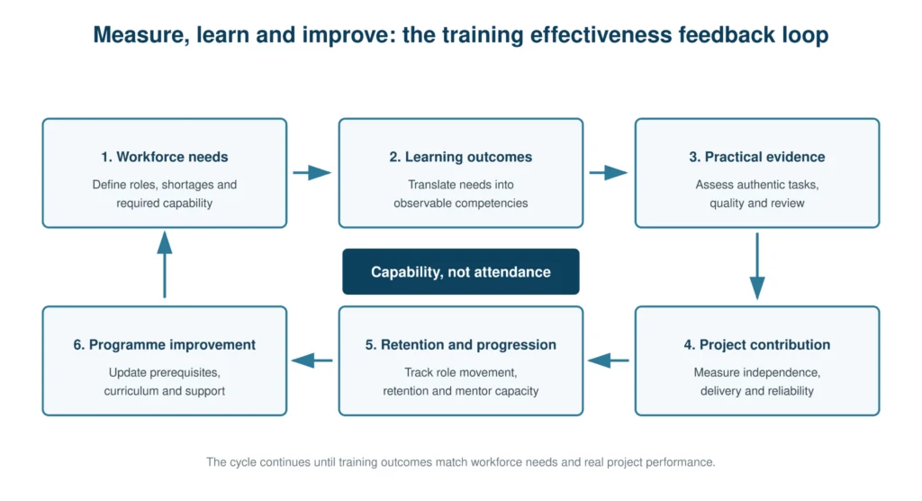
Figure 3: Effective training uses a closed feedback loop from workforce needs to curriculum improvement. [5]
Building Stronger Collaboration Across Industry, Academia and Professional Communities
No single employer or university can close the semiconductor skills gap independently. Universities understand education, research and long-term capability. Employers understand live project needs and commercial constraints. Training providers can create focused pathways. Professional communities can expose engineers to methods and experience outside their immediate teams.
| Collaboration mechanism | What partners should do | Expected benefit |
| Shared competency frameworks | Define foundation, applied and advanced capability across roles | Clearer curricula, recruitment and progression |
| Industry-informed curricula | Review workflows, examples, failure modes and assessment | Better alignment without tying courses to one employer |
| Shared laboratories | Provide regional EDA, FPGA, measurement and fabrication access | Wider participation and reduced duplication |
| Placements and internships | Set learning goals, supervision and useful technical work | Earlier career visibility and practical evidence |
| Technical communities | Share methods, case studies and emerging practice | Continuing professional development and knowledge transfer |
Table 4: Practical collaboration mechanisms
The UK AI Hardware Plan also proposes collaboration between government, employers, education providers and industry partners to strengthen chip design and verification pathways. [4] Collaboration becomes useful when roles, resources and measurable outcomes are explicit.
Alpinum’s DVClub events cover processor verification, RISC-V, formal methods, security and AI in design verification. The Verification Futures conferences provide another forum for engineers, researchers, EDA providers and technical leaders to exchange practical experience.
How Alpinum’s Courses and Conferences Support Continuing Skills Development
Closing the semiconductor skills gap requires connected forms of development. Universities need resources that help students apply academic foundations. Employers need pathways for new recruits and engineers moving between domains. Practising engineers need continuing access to specialist methods and professional communities.
Alpinum’s semiconductor verification training portfolio covers SystemVerilog, UVM, formal verification, RISC-V, low-power verification, AMS, FPGA, embedded software and AI-assisted verification. Delivery options include online, live, hybrid, on-demand and team-based formats. Practical exercises, quizzes and controlled tool environments help participants apply the material.
Selected university students can access reduced-price places on eligible programmes through academic-email verification. This supports early-career engineers who need practical experience in verification, UVM, formal methods and RISC-V.
Courses alone are not sufficient. Engineers also need to hear how other teams approach architecture, implementation, verification, AI adoption and sign-off. DVClub and Verification Futures connect universities, employers, tool providers and practising engineers through technical presentations and discussion.
Capability before certificates
The objective is not to produce engineers who know one language or methodology in isolation. It is to develop the understanding, practical evidence and judgement required to contribute to complex semiconductor programmes.
Conclusion
The semiconductor skills gap in 2026 is not simply a shortage of applicants. It is a capability-development challenge shaped by industry growth, system complexity, retirement, limited practical exposure and global competition for experienced people.
Universities can respond by combining strong academic foundations with industry-informed projects, verification education, interdisciplinary work and accessible tool environments. Employers can respond with structured early-career programmes, realistic skills-based recruitment, visible technical career paths, apprenticeships, protected learning and recognised mentoring responsibilities.
Professional communities and training providers can connect these efforts through practical exercises, shared methods and continuing development. The next generation of semiconductor engineers will be built through repeated cycles of learning, application, review, mentoring and increasing technical responsibility.
Organisations building capability across design, verification, formal methods, software, RISC-V and AI-assisted workflows can review Alpinum’s practical semiconductor training programmes and technical events.
References
[1] Department for Science, Innovation and Technology, “Semiconductor Sector Study 2026,” UK Government, Jun. 12, 2026. [Online]. Available: https://www.gov.uk/government/publications/semiconductor-sector-study-2026/semiconductor-sector-study-2026.
[2] Department for Science, Innovation and Technology, “UK semiconductor workforce study: Executive summary,” UK Government, Apr. 30, 2025. [Online]. Available: https://www.gov.uk/government/publications/uk-semiconductor-workforce-study/uk-semiconductor-workforce-study-executive-summary.
[3] SEMI Europe, “Bridging Europe’s chip talent gap: How the European Chips Skills Academy is leading the way,” Dec. 2025. [Online]. Available: https://www.semi.org/en/blogs/bridging-europes-chip-talent-gap-how-the-european-chips-skills-academy-ecsa-is-leading-the-way.
[4] Department for Science, Innovation and Technology, “UK AI Hardware Plan,” UK Government, Jun. 8, 2026. [Online]. Available: https://www.gov.uk/government/publications/uk-ai-hardware-plan/uk-ai-hardware-plan.
[5] National Institute of Standards and Technology, “CHIPS R&D Education and Workforce Development Plan Guidebook,” May 29, 2025. [Online]. Available: https://www.nist.gov/document/chips-rd-education-and-workforce-development-ewd-plan-guidebook.
[6] Semiconductor Industry Association and Oxford Economics, “Chipping Away: Assessing and Addressing the Labor Market Gap Facing the U.S. Semiconductor Industry,” 2023. [Online]. Available: https://www.semiconductors.org/chipping-away-assessing-and-addressing-the-labor-market-gap-facing-the-u-s-semiconductor-industry/.
[7] Council for Science and Technology, “Advice on building a sovereign AI chip design industry in the UK,” UK Government, Aug. 21, 2025. [Online]. Available: https://www.gov.uk/government/publications/building-a-sovereign-ai-chip-design-industry-in-the-uk/council-for-science-and-technology-advice-on-building-a-sovereign-ai-chip-design-industry-in-the-uk.
[8] S. Freeman et al., “Active learning increases student performance in science, engineering, and mathematics,” Proc. Natl. Acad. Sci. USA, vol. 111, no. 23, pp. 8410–8415, 2014, doi: https://doi.org/10.1073/pnas.1319030111.
[9] Accellera Systems Initiative, “UVM standard and reference implementation resources.” [Online]. Available: https://www.accellera.org/downloads/standards/uvm.
FAQs
It is the difference between the technical capabilities semiconductor organisations require and the number of people who currently possess those capabilities. It covers design, verification, embedded software, manufacturing, process engineering, packaging, test and technical leadership
Semiconductor activity and system complexity are increasing while many experienced specialists are approaching retirement. Universities also produce fewer graduates with practical semiconductor experience than employers need.
Important capabilities include digital and analogue design, SystemVerilog and UVM, formal verification, embedded software, physical implementation, RISC-V, processor verification, advanced packaging, manufacturing, post-silicon validation and hardware security.
Graduates often have valuable theoretical foundations but limited experience with specifications, EDA tools, verification planning, regressions, code reviews and hardware-software integration. Universities and employers share responsibility for closing this transition gap.
Universities can introduce semiconductor contexts earlier, teach verification as a core discipline, use industry-reviewed capstone projects, provide remote tool access, support staff development and strengthen placements.
Employers should use staged onboarding, practical exercises, supervised project work, mentoring, rotations and clear competency targets. Responsibility should grow as evidence and independence improve.
Yes. Well-designed apprenticeships can expand access to technician, manufacturing, test, software-support and selected engineering roles. They need paid learning, qualified supervision, progressive responsibility and recognised competencies.
AI may reduce repetitive work and support coding, regression analysis, assertion development and knowledge retrieval. It does not remove the need to understand requirements, review evidence, manage risk and make sign-off decisions.
Use practical assessments, quality of work, time to independent contribution, project performance, retention and progression. Attendance and certificates are useful administrative measures, but they do not prove capability.
Begin with digital logic, architecture and programming, then progress through SystemVerilog, assertions, coverage, UVM, planning, regressions and debug. Practical exercises should accompany every stage.

Written by : Mike Bartley
Mike started in software testing in 1988 after completing a PhD in Math, moving to semiconductor Design Verification (DV) in 1994, verifying designs (on Silicon and FPGA) going into commercial and safety-related sectors such as mobile phones, automotive, comms, cloud/data servers, and Artificial Intelligence. Mike built and managed state-of-the-art DV teams inside several companies, specialising in CPU verification.
Mike founded and grew a DV services company to 450+ engineers globally, successfully delivering services and solutions to over 50+ clients.
Mike started Alpinum in April 2016 to deliver a range of start-of-the art industry solutions:
Alpinum AI provides tools and automations using Artificial Intelligence to help companies reduce development costs (by up to 90%!) Alpinum Services provides RTL to GDS VLSI services from nearshore and offshore centres in Vietnam, India, Egypt, Eastern Europe, Mexico and Costa Rica. Alpinum Consulting also provides strategic board level consultancy services, helping companies to grow. Alpinum training department provides self-paced, fully online training in System Verilog, UVM Introduction and Advanced, Formal Verification, DV methodologies for SV, UVM, VHDL and OSVVM and CPU/RISC-V. Alpinum Events organises a number of free-to-attend industry events
You can contact Mike (mike@alpinumconsulting.com or +44 7796 307958) or book a meeting with Mike using Calendly (https://calendly.com/mike-alpinum-consulting).
Stay Informed and Stay Ahead
Latest Articles, Guides and News
Explore related insights from Alpinum that dive deeper into design verification challenges, practical solutions, and expert perspectives from across the global engineering landscape.