
On 17 September 2026, Applied Materials said it plans to invest $5 billion in India over the next decade, announcing the commitment as SEMICON India 2026 opened in New Delhi. Reuters reported that the investment will centre on research, supply-chain scale-up and workforce growth. Applied supplies semiconductor manufacturing equipment and services rather than finished chips, so the Applied Materials India investment is not directly about chip design or verification.
It does, however, raise a question that will outlast the headline number: as semiconductor investment and manufacturing capability expand in India, which design, verification, software and AI-assisted engineering capabilities will companies need to turn that investment into working silicon? This article separates reported facts from engineering implications and focuses on that capability question.
What does Applied Materials’ $5B India investment mean for semiconductor engineering skills?
| Applied Materials plans to invest $5 billion in India over the next decade, centred on research, supply-chain scale-up and workforce growth. The announcement most directly concerns semiconductor equipment R&D, supply-chain capability and workforce development. As India’s ecosystem deepens, it is likely to increase demand for chip design, verification, embedded software, validation, advanced packaging, EDA and AI-assisted engineering skills as well. That wider effect is an implication, not a stated commitment. |
What Did Applied Materials Announce at SEMICON India 2026?
Applied announced the planned $5 billion investment over ten years on 17 September 2026. Indian coverage has described the programme as India Vision 2035. Prabu Raja, president of Applied’s Semiconductor Products Group, described three priorities: deepen R&D in India, accelerate the domestic ecosystem and develop future talent. ANI reported a planned 140-acre advanced semiconductor research park and a target to expand India-based supply-chain capacity tenfold by 2035.
The plan builds on an existing base. In a February 2026 post, Applied Materials’ newsroom described a new Bengaluru campus of more than 800,000 sq ft, an India Validation Center that the company says is the country’s only facility capable of processing 300mm wafers, and an AI Center of Excellence in Chennai.
SEMICON India 2026 ran from 17 to 19 September at Yashobhoomi, New Delhi, organised by SEMI with the India Semiconductor Mission and MeitY. SEMI said the event would feature more than 500 exhibitors from over 40 countries, while the government’s pre-event note cited more than 600 companies and 52 countries. At the opening, the Prime Minister announced a $13.5 billion second phase of the Semiconductor Mission. The Cabinet had already approved Semicon 2.0 in July 2026 with an outlay of Rs 1,27,500 crore across design, machines and materials, fabs, packaging, R&D and talent.
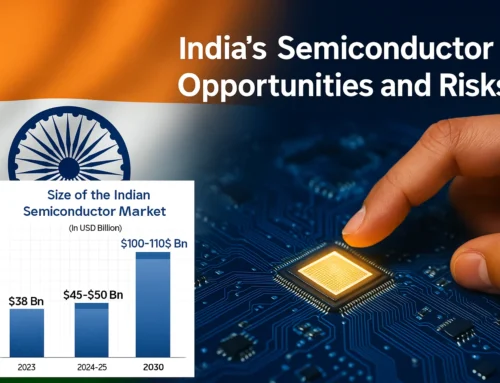
For the wider policy, investment and ecosystem context, see Alpinum’s analysis of India’s semiconductor opportunities and risks.
Details still to watch: the year-by-year phasing of the $5 billion commitment, the research park’s final location and timeline, and progress against the 2035 targets.
Why This Matters Beyond the Investment Number
Capital creates conditions; engineering capability turns those conditions into products. A useful way to read the announcement is as the first link in a longer chain:
Investment -> infrastructure -> manufacturing and process capability -> chip design -> verification -> embedded software -> validation -> skilled workforce -> repeatable product delivery
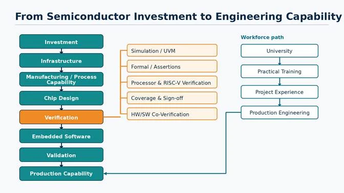
Figure 1. Investment creates the conditions for semiconductor capability. Engineers who can design, verify, validate and support silicon turn those conditions into production capability. Source: Alpinum analysis.
Each link depends on the ones before it, but none of the later links is automatic. A research park or a larger supplier base does not by itself produce a verified SoC. A functional bug discovered after fabrication can require costly workarounds and, in serious cases, a silicon respin with additional mask, schedule and engineering cost. Among respondents to the 2024 Wilson Research Group study, 14% of IC/ASIC projects achieved first-silicon success; Siemens EDA described that as the lowest level in two decades.
Design and verification maturity therefore influences how much value new infrastructure can capture. Applied itself lists future talent as a priority; the engineering question is which capabilities are needed, at what depth, and how repeatably teams can apply them.
India Already Has a Strong Chip-Design Base
India’s semiconductor ecosystem starts from significant design strength. According to a Press Information Bureau update from March 2026, India hosts about 7% of the world’s semiconductor-domain global capability centres and employs nearly 20% of the global chip-design workforce. The Design Linked Incentive scheme had approved 24 chip and SoC design projects; 105 fabless companies had received design-infrastructure support; 315 universities had access to advanced EDA tools; and 146 student designs from 49 institutions had taped out.
At SEMICON India 2026, the Prime Minister said about 70,000 people had already been trained in chip design, while Ashwini Vaishnaw said Semicon 2.0 would target at least 200 startups and companies designing chips in India. Business Standard reported the design-company target.
Scaling domestic design, packaging and manufacturing activity changes the kind of capability that must be available repeatedly across projects. Breadth of design talent is already a strength. The next test is depth and repeatability in verification sign-off, formal methods, processor verification and hardware/software validation.
Six Engineering Capabilities India Will Need as Semiconductor Investment Scales
The following areas are engineering priorities rather than job forecasts. They describe capabilities that become increasingly important as investment is converted into products.
1. Digital Design and RTL Engineering
Manufacturing capacity matters only if competitive designs are available to build. RTL engineers translate architecture into implementable logic, typically using SystemVerilog, while accounting for synthesis, timing, low-power intent and IP integration. As local fabrication and packaging capability grows, engineers who understand how architectural choices affect timing closure, power and integration risk can connect design decisions more effectively to downstream implementation.
2. Design Verification and UVM
Design verification builds evidence that a design behaves according to its specification before fabrication. Simulation-based flows use SystemVerilog and UVM, constrained-random stimulus, assertions and functional coverage, guided by a verification plan. Regressions support coverage closure against defined sign-off criteria. What scales is not tool familiarity alone, but reusable verification environments, disciplined debug and a clear connection between verification intent and evidence. See Alpinum’s Design Verification for SystemVerilog/UVM Training.
3. Formal Verification
Formal verification uses mathematical analysis to prove or refute selected properties within a formal model and its stated assumptions. It is well suited to connectivity, control logic, protocol behaviour, deadlock and forward-progress conditions, security properties and corner cases that simulation may reach only rarely. Formal complements simulation rather than replacing it, and it requires skill in writing meaningful properties, constraining the environment correctly and judging proof completeness. See Alpinum’s Formal Verification Training.
4. RISC-V and Custom Processor Verification
Open processor architectures allow teams to develop custom processors and accelerators for embedded, automotive, industrial and AI workloads. That increases verification responsibility. ISA conformance, privilege architecture, memory behaviour and interrupts can be checked against architectural specifications and reference models, while custom extensions require verification against their defined specification and an appropriately extended reference model. See Alpinum’s RISC-V Verification Training.
5. Embedded Software and Hardware/Software Validation
For software-controlled SoCs and processors, silicon is not a deployable product until firmware and software run reliably on it. Boot flows, drivers, RTOS ports, interrupts and memory-mapped interfaces need to be validated against the hardware. Emulation and FPGA prototyping can bring software into the verification process before silicon returns, followed by system testing and, where relevant, functional-safety practice. See Alpinum’s Embedded Software Testing services.
6. AI-Assisted Engineering
Engineers are increasingly using AI assistance for bounded tasks such as coding, test generation, log analysis and specification retrieval. Retrieval-augmented generation (RAG), Model Context Protocol (MCP) integrations and engineering agents can improve workflow efficiency, but they do not remove the need for review, verification or sign-off. Alpinum’s India-focused AI-Assisted Coding, RAG, MCP and Agentic AI Training addresses these controlled engineering workflows.
Semiconductor skills matrix
| Area | Essential skills | Why it matters |
| RTL design | SystemVerilog, microarchitecture, synthesis and timing awareness | Converts architecture into implementable logic |
| Design verification | SV/UVM, assertions, functional coverage, verification planning | Builds evidence of functional correctness before silicon |
| Formal verification | SVA, property checking, assumptions, proof analysis | Proves selected properties and exposes hard-to-reach corner cases |
| RISC-V | ISA, privilege architecture, memory systems, extensions | Supports custom processor verification |
| Embedded | C/C++, Python, RTOS, drivers, HW/SW integration | Connects silicon to deployable systems |
| AI-assisted engineering | RAG, MCP, agents, prompt discipline, output review | Improves productivity under engineering control |
From Manufacturing Capacity to Verification Capacity
A useful test for any semiconductor investment is which capability it strengthens directly and which capabilities still need to be built through engineering programmes. Applied’s plan primarily strengthens equipment R&D, supply-chain foundations and the workforce base that support manufacturing capacity. Design, verification, software and validation capacity must still be built through projects, tools, processes and experienced teams.
| Capability | Core question |
| Manufacturing capacity | Can the ecosystem manufacture and package devices repeatably? |
| Design capacity | Can teams architect and implement competitive silicon? |
| Verification capacity | Can teams build sufficient evidence that complex designs satisfy their requirements? |
| Software capacity | Can firmware and software use the hardware reliably? |
| Validation capacity | Can complete systems be tested under realistic conditions? |
| Skills capacity | Can the ecosystem scale these disciplines across enough engineers and projects? |
For verification capability specifically, Alpinum’s pre-silicon verification work illustrates the type of engineering discipline required before silicon is committed.
Why Verification Skills Become More Important as Designs Become More Complex
Modern SoCs can combine heterogeneous compute, AI accelerators, custom processor extensions, chiplets, security features, multiple low-power modes and tightly coupled software. Additional blocks, operating modes, power domains and configurations can multiply the interactions that must be verified. The state space can grow combinatorially, making exhaustive simulation impractical for non-trivial SoCs and forcing verification teams to plan, prioritise and measure their evidence.
- Simulation and UVM provide broad functional exploration and coverage against verification intent
- Formal verification can exhaustively analyse selected properties within a defined model and set of assumptions
- Emulation supports realistic software workloads and long-running scenarios before silicon
- FPGA prototyping provides higher execution speed for software development and system exploration
- Post-silicon and embedded validation exercise real firmware and hardware during bring-up and system testing
The engineering skill lies in choosing the right mix and understanding what each result does and does not prove. Verification capability is less visible than manufacturing capacity, but it requires sustained project experience to build and scale.
What SEMICON India 2026 Signals for Engineers and Employers
SEMICON India 2026 included a Workforce Development Pavilion and a Student Hackathon. Against that backdrop, several capability priorities stand out for different audiences.
For engineers
Useful technical depth includes RTL and SystemVerilog, UVM, formal verification, RISC-V, embedded software, Python, verification planning, system validation and AI-assisted engineering. A valuable profile combines depth in one discipline with working knowledge of adjacent areas, supported by project evidence rather than certificates alone.
For semiconductor employers
Capability is built through structure: staged upskilling, practical labs on representative designs, project-based learning, independent review and clear sign-off standards. A practical maturity path is:
| Stage | What happens | Evidence of readiness |
| Learn | Concepts, languages and methodology | Can explain and apply core ideas |
| Practise | Guided labs on representative designs and tools | Completes realistic labs with decreasing support |
| Apply | Project work with planning, implementation and coverage | Delivers project evidence against defined objectives |
| Verify | Independent review of results, gaps and AI-generated output | Can defend results and identify what remains unproven |
| Sign-off | Accountable decision supported by documented evidence | Can own or contribute to a defined sign-off criterion |
For universities
Tool access is spreading, with PIB reporting 315 universities using advanced EDA tools. The next step is workflow depth: curricula aligned with real verification and hardware/software flows, practical project experience and exposure to industry methodology and controlled AI-assisted development. Universities exploring industry-aligned access can read about Alpinum’s University Student Access Programme.
Semiconductor Jobs in India: Which Roles Could Benefit?
This article does not forecast job numbers. The roles below are those most directly connected to the capability chain described above. For the broader workforce picture, see Alpinum’s semiconductor skills gap analysis.
| Role | Differentiating skill combination |
| RTL design engineer | SystemVerilog plus timing, power and IP-integration awareness |
| Design verification engineer | UVM plus verification planning, coverage analysis and debug |
| Formal verification engineer | Property writing, assumption management, proof analysis and coverage |
| RISC-V verification engineer | ISA and privilege knowledge, reference-model comparison, custom-extension verification |
| FPGA engineer | RTL plus prototyping, timing closure and on-hardware debug |
| Embedded software engineer | C/C++, RTOS, drivers and bring-up on new silicon |
| Validation engineer | System-level test design, HW/SW integration and failure analysis |
| Semiconductor test engineer | Test strategy, production-test constraints and Python data analysis |
| AI-assisted engineering roles | Workflow design, RAG, tool integration, review discipline and governance |
Engineers who combine a core discipline with an adjacent capability, such as UVM with formal methods or embedded software with hardware validation, can operate more effectively across project boundaries.
AI Will Change the Skills Mix, Not Remove the Need for Verification
Whether AI is applied in manufacturing, design or verification, the central engineering requirement is the same: use AI within bounded workflows and verify the outputs before they influence sign-off. Applied’s Chennai AI Center of Excellence provides a manufacturing-side example of advanced analytics and AI supporting high-volume operations. In design and verification, current industry work increasingly combines generative or agentic assistance with deterministic EDA tools and reference models.
Rather than duplicate Alpinum’s existing AI-skills guidance here, see the dedicated guide to the skills semiconductor engineers need to use AI effectively and Alpinum’s AI in Design Verification work for the deeper treatment.
What Should Engineering Leaders in India Prioritise Now?
- Where are our verification capability gaps by block, protocol and project stage?
- Do engineers understand both simulation and formal methods, including the limits of each?
- Can teams verify RISC-V or custom processor architectures, including defined extensions?
- Are hardware and software teams trained to validate systems together?
- Can AI-assisted engineering be used with review, traceability and appropriate governance?
- Do engineers understand coverage and sign-off, not just tool operation?
- Are training programmes aligned with realistic project workflows?
- Can capability scale across future programmes, or does it depend on a few individuals?
Alpinum Perspective
Infrastructure investment and engineering skills need to progress together. Alpinum works on the engineering side of that equation through practical training and consulting in SystemVerilog/UVM, formal verification, RISC-V verification, embedded software testing and AI-assisted engineering. Verification capability is one link in the chain, not the whole of it: manufacturing, product strategy, software, supply chains and capital matter too.
Building Semiconductor Engineering Capability in India
As investment in India’s semiconductor ecosystem grows, organisations also need engineers equipped for increasingly complex design, verification and software workflows. Alpinum provides practical training across AI-assisted coding, formal verification, RISC-V verification, SystemVerilog/UVM and embedded engineering for individuals, universities and technical teams. Explore the Alpinum training portfolio.
References
1. Reuters / Yahoo Finance, 17 Sep 2026
2. ANI, Applied Materials announces USD 5 bn India investment, 17 Sep 2026
3. TechNode, Applied Materials commits $5B to expand India semiconductor footprint, 18 Sep 2026
4. Applied Materials, A New Chapter for Applied Materials India, 5 Feb 2026
5. SEMI, SEMICON India 2026 event announcement
6. Prime Minister of India, SEMICON India 2026 pre-event note
7. Prime Minister of India, SEMICON India 2026 inauguration
8. Press Information Bureau, Cabinet approves Semicon 2.0, 15 Jul 2026
9. Press Information Bureau, India semiconductor design and R&D update, 13 Mar 2026
10. Business Standard, Semicon 2.0 design startup target, 17 Sep 2026
11. Siemens EDA, 2024 Wilson Research Group IC/ASIC Functional Verification Trend Report
12. Siemens, self-verifying agentic AI workflows for semiconductor and PCB design, 26 Jul 2026
13. IEEE Spectrum, AI Agent Designs a RISC-V CPU Core From Scratch, 22 Apr 2026
FAQs
Applied Materials plans to invest $5 billion in India over the next decade, announced on 17 September 2026 at SEMICON India 2026. Reported priorities centre on research, supply-chain scale-up and workforce growth, alongside a planned advanced semiconductor research park.
The direct announcement concerns semiconductor equipment R&D, supply-chain capability and workforce development. The effect on chip design and verification is indirect and depends on how design, software, validation and engineering capability grow alongside manufacturing infrastructure.
More semiconductor activity creates more design starts, integrations, software stacks and system-validation work. That increases the importance of repeatable verification planning, UVM, formal methods, processor verification, embedded validation and clear sign-off evidence.
Relevant capabilities include RTL and SystemVerilog, UVM, formal verification, RISC-V and processor verification, embedded software, system validation, Python and controlled AI-assisted engineering. Manufacturing roles also require process and equipment expertise.
Yes, particularly where teams develop custom processors or extensions. Verification must cover ISA behaviour, privilege modes, memory and interrupt behaviour, integration and any custom functionality defined beyond the base architecture.
Look for practical programmes that combine methodology with realistic labs and project evidence. For verification-focused teams, useful areas include SystemVerilog/UVM, formal verification, RISC-V verification, embedded validation and controlled AI-assisted engineering.

Written by : Mike Bartley
Mike started in software testing in 1988 after completing a PhD in Math, moving to semiconductor Design Verification (DV) in 1994, verifying designs (on Silicon and FPGA) going into commercial and safety-related sectors such as mobile phones, automotive, comms, cloud/data servers, and Artificial Intelligence. Mike built and managed state-of-the-art DV teams inside several companies, specialising in CPU verification.
Mike founded and grew a DV services company to 450+ engineers globally, successfully delivering services and solutions to over 50+ clients.
Mike started Alpinum in April 2016 to deliver a range of start-of-the art industry solutions:
Alpinum AI provides tools and automations using Artificial Intelligence to help companies reduce development costs (by up to 90%!) Alpinum Services provides RTL to GDS VLSI services from nearshore and offshore centres in Vietnam, India, Egypt, Eastern Europe, Mexico and Costa Rica. Alpinum Consulting also provides strategic board level consultancy services, helping companies to grow. Alpinum training department provides self-paced, fully online training in System Verilog, UVM Introduction and Advanced, Formal Verification, DV methodologies for SV, UVM, VHDL and OSVVM and CPU/RISC-V. Alpinum Events organises a number of free-to-attend industry events
You can contact Mike (mike@alpinumconsulting.com or +44 7796 307958) or book a meeting with Mike using Calendly (https://calendly.com/mike-alpinum-consulting).
Stay Informed and Stay Ahead
Latest Articles, Guides and News
Explore related insights from Alpinum that dive deeper into design verification challenges, practical solutions, and expert perspectives from across the global engineering landscape.