Artificial intelligence is often discussed as a way to make engineers faster. That is useful, but it is not the most important question for semiconductor leaders.
The bigger question is this:
Can AI change what is possible within the same cost, schedule, scope and risk constraints?
Every semiconductor programme operates inside a delivery boundary. There is a limit to what can be achieved with the available budget, team capacity, specification maturity, schedule pressure and acceptable technical risk. Traditionally, changing one dimension usually affects the others. Increase the scope, and the programme may need more engineers, more time or more risk acceptance. Compress the schedule, and the team may need extra resources, a narrower specification or a higher tolerance for late-stage defects.
The cost–schedule–scope–risk relationship matters for semiconductor organisations because chip development is already under pressure from AI accelerators, automotive SoCs, chiplet-based architectures, advanced packaging, RISC-V adoption, FPGA prototyping, embedded software complexity and increasing verification expectations. For many teams, the challenge is not simply “how do we use AI?” The better question is, where can AI safely improve engineering capability without weakening design assurance or sign-off discipline?
That question aligns closely with Alpinum Consulting’s wider work across AI in design verification, semiconductor design and verification services, formal verification, RISC-V verification, FPGA services and embedded software testing.
AI does not magically remove engineering trade-offs. It does not make unclear specifications clear on its own. It does not prove a design is correct without evidence. It does not replace architecture judgment, verification strategy, review discipline or accountable sign-off.
However, AI can move the boundary.
Used properly, AI can help teams analyse change faster, reuse knowledge more effectively, identify risks earlier, automate repetitive investigations, accelerate design-space exploration, and improve planning decisions. The result is not a world without constraints. It is a world where semiconductor teams may be able to achieve more within the same constraints, or reach the same outcome with less uncertainty.
That distinction matters.
Key learning points
| Key learning point | Link to detailed explanation | External reference link |
| Semiconductor programmes operate within a four-dimensional delivery boundary consisting of cost, schedule, scope/specification and risk. Changes in one dimension usually affect the others. | The Old Engineering Rule: Change One Thing, Affect the Others | [1], [2] |
| AI does not eliminate engineering trade-offs, but it can move the feasible delivery boundary by reducing uncertainty, improving reuse and enabling faster decision-making. | The Four-Dimensional Delivery Boundary | [2], [3], [4] |
| The greatest value of AI in semiconductor engineering comes from practical workflows such as requirements analysis, regression triage, coverage review, debug support and knowledge retrieval. | How AI Can Move the Boundary | [3], [4], [5] |
| Semiconductor teams should measure AI adoption using engineering outcomes such as reduced debug effort, earlier risk discovery and improved sign-off confidence rather than simple productivity metrics. | The Risk of Moving Faster Without Moving the Boundary | [5], [6] |
| Successful AI adoption requires a capability-led approach focused on governance, traceability, workflow integration and measurable improvement rather than tool-driven experimentation. | A Practical Framework for AI Adoption | [1], [5], [6] |
The old engineering rule: change one thing, affect the others
In engineering delivery, cost, schedule, scope and risk are connected.
If the scope increases, the project usually requires more cost, more time, or greater risk acceptance. If the schedule is shortened, the team may need more people, better automation, reduced scope or a higher level of residual risk. If cost is fixed, the team may need to reduce ambition, extend the schedule or accept constraints on verification depth. For that reason, engineering delivery is not simply a planning exercise. It is a constraint-management problem.
For a semiconductor programme, the four dimensions can be understood as follows:
| Dimension | What does it mean in semiconductor engineering | Typical pressure point |
| Cost | Engineering effort, tools, licences, compute, specialist support, IP, verification capacity, FPGA prototyping, embedded software validation and management overhead. | Budget limits, tool costs, resource availability and specialist engineer scarcity. |
| Schedule | Time to architecture freeze, RTL readiness, verification milestones, physical design, embedded software readiness, sign-off and tape-out. | Market windows, customer deadlines, conference launches, funding milestones and tape-out commitments. |
| Scope/specification | Required features, interfaces, protocols, performance targets, safety/security requirements, software-visible behaviour and compliance expectations. | Late changes, unclear requirements, expanding customer needs and interface complexity. |
| Risk | Functional bugs, missed requirements, insufficient coverage, integration failures, respins, safety exposure, firmware issues and commercial risk. | Late defect discovery, weak sign-off confidence, poor traceability and incomplete verification closure. |
The traditional assumption is that these dimensions are tightly coupled. Move one, and one or more of the others must move too. That assumption is mostly true. But it is not the whole story.
The reason AI is strategically interesting is that it may improve the way teams move within this constraint space. It may reduce wasted effort, expose hidden dependencies, support better prioritisation and improve the timing of decisions. In other words, AI can help teams move the feasible delivery boundary, not by removing engineering reality, but by reducing avoidable friction.
Because AI’s real value lies in improving engineering decision-making rather than replacing engineering judgment, the debate around whether AI will replace semiconductor engineers is often framed too narrowly. The more useful question is whether AI can help experienced engineers make better decisions, reduce repetitive work and focus more time on architecture, review, verification quality and risk control.
Why does this matter more in semiconductor programmes?
The cost–schedule–scope–risk relationship exists in all engineering domains, but semiconductor projects feel it more sharply. A software defect can often be patched. A silicon defect may require a costly workaround, a firmware mitigation, a delayed launch or a respin. Verification is also not a single activity at the end of the programme. It is a continuous evidence-building process spanning requirements, architecture, design, testbench development, regression, debugging, coverage closure, formal analysis, and sign-off.
That is why effective verification planning to coverage closure remains central to delivery confidence. A plan that does not connect requirements, features, tests, coverage and review evidence can easily create false confidence. AI may accelerate parts of the workflow, but it does not remove the need for structured verification intent.
Modern chip programmes are also becoming more complex. AI accelerators, automotive SoCs, RISC-V designs, chiplet-based systems, advanced packaging, FPGA platforms and safety-critical systems all increase the pressure on engineering teams. For example, RISC-V verification introduces challenges related to configurability, extensions, instruction behaviour, privilege modes, compliance, coverage, and software interaction. Similarly, chiplet-based systems raise new questions about system-level verification, interoperability, package-level behaviour, test strategy, and integration risk.
At the same time, embedded and firmware complexity is becoming more central to product behaviour. A silicon team may achieve RTL closure, but a product can still be delayed if embedded software, drivers, boot flows, safety monitoring, diagnostics or validation environments are not ready. These hardware/software dependencies are where embedded software development and automotive embedded software testing become part of the same delivery-risk conversation.
In this environment, AI should not be treated as a shortcut around the engineering discipline. In semiconductor delivery, the real value of AI is not simply in its ability to produce more output. The value is that it can help teams make better decisions earlier, with clearer evidence and less wasted effort.
The four-dimensional delivery boundary
A useful way to think about semiconductor programme delivery is to view it as a four-dimensional boundary. Inside the boundary, the programme is feasible. The team has sufficient time, budget, resources, clarity of specifications, and risk control to achieve a credible outcome. Outside the boundary, the programme becomes unsafe, unrealistic or commercially exposed.
The boundary can move in two directions.
- It can shrink when the project becomes harder: unclear requirements, late feature changes, tool bottlenecks, poor reuse, weak planning assumptions, insufficient verification strategy, unmanaged FPGA prototype complexity, embedded software delays or unexpected integration issues.
- It can expand when the team improves its capabilities: better automation, stronger reuse, earlier risk identification, clearer requirements management, faster debugging, improved verification planning, stronger formal methods, better decision support, and more effective engineering leadership.
The ability to expand the delivery boundary is where AI becomes important.
AI can move the boundary by improving the team’s ability to understand, predict, investigate, and act. It cannot move the boundary when it only generates more artefacts without improving engineering confidence. A team that uses AI to create unreviewed code, tests, reports or plans may simply move faster towards uncertainty. A team that uses AI to improve traceability, highlight the impact of change, prioritise debugging, and support measurable verification outcomes may genuinely improve delivery capability.
That distinction separates AI as activity generation and AI as an engineering capability.
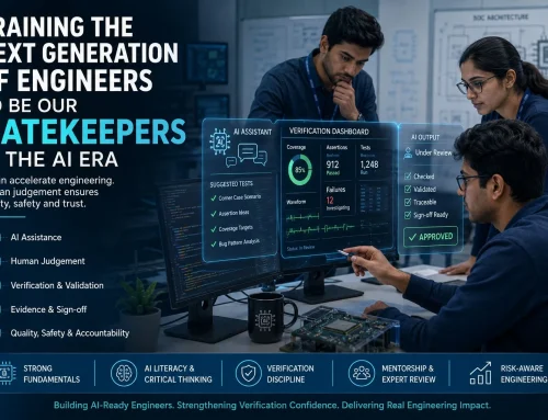
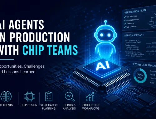
Alpinum’s work on AI in DV safe pilot adoption is especially relevant here. The right starting point is not to automate everything. The right starting point is to choose bounded, reviewable, and measurable workflows in which AI can support engineers without weakening accountability.
How AI can move the boundary
AI can help semiconductor teams in several practical ways.
1. Faster impact analysis when scope changes
Late scope changes are one of the most common causes of delivery pressure. A new interface, protocol update, safety requirement, power mode, performance target, or customer-specific feature can affect the architecture, RTL, verification plans, testbenches, coverage models, embedded software, FPGA prototypes, documentation, and sign-off evidence.
Traditionally, impact analysis relies heavily on expert review. That remains necessary, but AI can help accelerate the first pass. AI can compare requirements, summarise design documents, identify affected modules, highlight potentially impacted tests, search historical issues and suggest areas where verification plans may need updating. AI-assisted impact analysis does not remove expert review, but it can reduce the time needed to understand the shape of the change.
In cost–schedule–scope–risk terms, this means that a scope change does not necessarily result in the same level of schedule delay or unmanaged risk. AI can help the team see the consequences earlier. For teams that offer or use semiconductor design and verification services, this is valuable because the impact of change is rarely limited to a single discipline. A specification update can affect RTL, UVM components, assertions, coverage, formal properties, firmware, documentation and customer acceptance evidence.
2. Better use of existing knowledge and reusable assets
Semiconductor organisations often have valuable knowledge distributed across previous projects, verification plans, bug databases, design reviews, scripts, testbenches, coverage reports, FPGA environments and internal documentation. The problem is that this knowledge is not always easy to find or reuse.
AI can help teams retrieve and apply prior knowledge more effectively. It can support documentation search, summarise historical bugs, identify reusable verification components, compare old and new specifications and help engineers understand why similar issues occurred in previous programmes.
AI-assisted knowledge retrieval is particularly useful where teams face resource constraints. AI does not replace experienced engineers, but it can reduce the time engineers spend searching for context or recreating work that already exists. The same knowledge-reuse benefit applies strongly to FPGA services, where teams may need fast prototyping, acceleration, validation environments or hardware/software integration support. It also applies to design verification training because teams with a more reusable methodology and stronger SystemVerilog/UVM foundations are better positioned to benefit from AI-assisted workflows.
3. Earlier risk detection
Risk is most expensive when it is discovered late.
A missed requirement near tape-out, a coverage gap found after regression closure, a protocol misunderstanding discovered during integration, a formal proof limitation discovered too late or an embedded software issue revealed after hardware assumptions are fixed can create significant schedule and cost pressure.
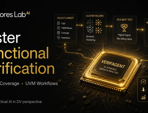
AI can help move some of this risk discovery earlier. It can review requirements for ambiguity, cluster failure patterns, summarise regression trends, highlight recurring bug signatures, assist with coverage gap analysis, and identify areas where verification evidence is thin. Earlier risk detection is especially relevant to AI in design verification. The strongest early use cases are often bounded and reviewable: regression triage, log summarisation, failure clustering, coverage review, documentation search and debug assistance.
AI can also support the adoption of stronger verification methods. For example, teams exploring strategic issues in adopting formal verification often face questions around property selection, proof convergence, scope definition, review effort and management confidence. AI cannot prove correctness on its own, but it may help engineers organise assumptions, review documentation, identify candidate properties, and connect formal evidence to wider verification planning.
4. Improved planning and resource allocation
Project planning often suffers because teams make decisions with incomplete information. Schedules are created before all technical risks are visible. Resource estimates are made before the full verification challenge is understood. Programme assumptions become fixed before the specification is stable.
AI can support planning by analysing historical effort, identifying recurring bottlenecks, summarising open risks, mapping dependencies and helping leaders understand where resource pressure is likely to appear. AI-supported planning does not make plans perfect. But it can make planning more evidence-based. For example, if AI-assisted analysis shows that a late interface change affects more tests, documentation and coverage points than expected, managers can respond earlier. They can adjust milestones, add specialist support, reduce lower-priority scope or strengthen verification focus before the schedule is already in trouble.
This type of planning support is particularly important for organisations balancing internal teams, external specialists, verification training, RISC-V programmes, FPGA prototyping and embedded software validation.
5. Faster design-space exploration
In some areas of chip design, AI can help explore alternatives faster than manual iteration alone. AI-powered EDA is already being positioned around design-space exploration, power/performance/area optimisation, automation and faster iteration. Faster design-space exploration matters because many engineering decisions are trade-offs. A team may need to compare architecture options, performance targets, power budgets, layout constraints, FPGA implementation choices, embedded software dependencies or verification approaches. AI can help generate options, rank alternatives, identify likely bottlenecks and reduce manual exploration effort.
The engineering decision still belongs to the team. But AI can improve the quality and speed of the decision process.
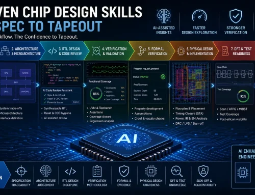
For individual engineers, this also changes the conversation about skills. The most valuable engineers will not simply be those who can prompt tools. They will be those who understand design intent, verification strategy, risk, evidence and review. As AI becomes part of the engineering workflow, topics such as AI-driven chip design skills from specification to tape-out, and how semiconductor engineers can learn AI and machine learning are becoming increasingly important.
Practical examples: how AI affects cost, schedule, scope and risk
| Situation | Traditional impact | How AI may help move the boundary | What still needs human engineering judgment |
| A customer adds a feature late in the programme | Scope increases, schedule slips or risk rises. | AI supports requirements comparison, impact analysis, document search, and identification of affected tests. | Engineers must confirm architectural impact, verification completeness and commercial trade-offs. |
| A tape-out date is fixed | The team may reduce scope, add cost, or accept higher risk. | AI helps prioritise debug, cluster failures, summarise regressions and identify high-risk areas. | Leaders must decide what evidence is sufficient for sign-off. |
| Budget is fixed | Scope or verification depth may be reduced. | AI improves reuse of existing scripts, test assets, documentation and historical lessons. | Reused assets still need validation in the new context. |
| Requirements are unclear | Rework and late defects become more likely. | AI can highlight ambiguity, inconsistency and missing acceptance criteria. | Domain experts must resolve intent with stakeholders. |
| Regression volume grows | Debug cost and schedule pressure increase. | AI summarises logs, clusters failures, and supports root cause investigation. | Engineers must verify the root cause and avoid false confidence. |
| New IP is integrated | Unknown behaviour increases risk. | AI helps search documentation, compare integration assumptions and review known issues. | Integration strategy and sign-off evidence remain engineering responsibilities. |
| Formal verification is introduced late. | The scope is unclear, proof targets may be poorly selected, and the review effort increases. | AI may help organise assumptions, review documents and connect formal targets to verification intent. | Formal experts must define the proof strategy and correctly interpret the results. |
| FPGA prototype complexity increases | Hardware/software integration and debug can become a bottleneck. | AI can help search logs, summarise failures and identify recurring integration patterns. | Engineers must confirm hardware behaviour, timing constraints and system-level validity. |
| Embedded software readiness is delayed | Product validation and customer delivery can slip even if RTL is ready. | AI can help organise test evidence, search documentation and support issue triage. | Firmware, driver and system validation decisions remain engineering-led. |
| Compliance or safety expectations increase | More documentation, review and verification effort required. | AI supports traceability, checklist review and evidence organisation. | Safety judgment, auditability and accountability cannot be delegated to AI. |
| Resource availability is limited | Delays or compromises in quality become more likely. | AI assists with repetitive analysis, reporting and knowledge retrieval. | Experienced engineers remain essential for architecture, review and decisions. |
The pattern is clear. AI helps most when it improves visibility, reduces repetitive effort and supports better decisions. It helps least when it is used to hide uncertainty or bypass review.
How AI can break the old rule, and where it cannot
The traditional rule states that if the scope increases, cost, schedule, or risk must increase as well. AI can sometimes weaken that relationship. For example, if AI reduces the time needed for impact analysis, documentation review, regression triage or coverage investigation, the team may be able to absorb some scope change without the same level of delay. But AI cannot completely break the rule.
If a new feature genuinely requires new architecture, RTL, verification strategy, safety analysis, embedded software work, FPGA validation, physical implementation work and customer validation, AI cannot make that work disappear. It can support the work. It can accelerate parts of the workflow. It can reduce avoidable waste. But the engineering substance remains. The limits of AI automation are why adoption must be framed around capability rather than hype.
A mature AI adoption strategy asks:
- Which workflows are bounded, repetitive and reviewable?
- Where is engineering time being wasted today?
- Which decisions are currently made too late?
- Where is risk hidden until the end of the programme?
- Which artefacts need better traceability?
- What evidence is required before AI-assisted output can be trusted?
- How will improvement be measured?
- Which design, verification, FPGA or embedded software workflows are suitable for safe AI pilots?
- Which workflows are too risky to automate without stronger governance?
These are not tool questions. They are engineering management questions. The same capability-led thinking is also why Alpinum’s wider “AI in DV” message is important. Successful AI adoption depends on governance, workflow integration, measurable pilots and human accountability, not simply buying more tools or generating more artefacts.
The risk of moving faster without moving the boundary
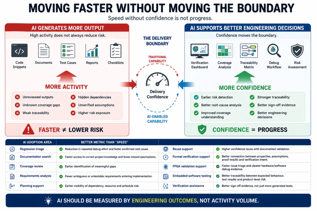
One danger of AI is that teams may confuse speed with progress. AI can generate summaries, scripts, code fragments, test ideas, documentation and reports very quickly. But if those outputs are not reviewed, traced, tested or connected to real engineering intent, they may increase risk rather than reduce it.
In semiconductor programmes, moving faster is only useful if confidence keeps pace.
A verification team that generates more tests but does not improve coverage understanding has not reduced risk. A design team that generates RTL faster but increases ambiguity has not improved delivery. A project team that produces more planning documents but does not expose hidden dependencies has not moved the boundary. A firmware team that creates more automated tests without understanding the hardware/software contract may still miss product-level failure modes.
AI should therefore be measured against engineering outcomes, not activity volume.
| AI adoption area | Better metric than “speed” |
| Regression triage | Reduction in repeated debugging effort and faster confirmation of the root cause. |
| Documentation search | Faster access to correct project knowledge and fewer missed assumptions. |
| Coverage review | Earlier identification of meaningful gaps. |
| Requirements analysis | Fewer ambiguous or untestable requirements are entering implementation. |
| Planning support | Earlier visibility of dependency, resource and schedule risk. |
| Reuse support | Higher confidence reuse with documented validation. |
| Formal verification support | Better connection between properties, assumptions, proof results and verification intent. |
| FPGA validation support | Faster issue triage and clearer hardware/software debug evidence. |
| Embedded software testing | Better traceability between expected behaviour, test results and product-level risk. |
| Verification assistance | Better sign-off evidence, not just more generated tests. |
These outcome-based measures show how AI moves from experimentation to measurable engineering capability. It is also where resources such as Verification Futures and DVClub are valuable. Industry discussion matters because AI adoption in engineering should be guided by practical experience, not only by tool marketing.
What this means for engineering leaders
For engineering leaders, the question should not be, “Which AI tool should we buy?”
The better question is:
Where is our current delivery boundary, and what would it take to move it safely?
That question forces a more useful discussion.
- If the main constraint is schedule, AI may help through accelerated debugging, automation, triage, planning support, and improved reuse.
- If the main constraint is cost, AI may help reduce wasted manual effort and improve knowledge reuse.
- If the main constraint is scope uncertainty, AI may help with requirements analysis, dependency mapping and change impact assessment.
- If the main constraint is risk, AI may help expose issues earlier, strengthen traceability and support evidence-based verification decisions.
Different programmes need different AI adoption strategies. A team building an automotive safety-critical SoC will have different needs from a team creating an FPGA prototype, an AI accelerator, a chiplet interconnect, a RISC-V subsystem, a mixed-signal product or an embedded software platform.
For example:
- A RISC-V team may need stronger instruction-level coverage, compliance confidence and configurable verification environments. Alpinum’s RISC-V verification training is relevant when teams need to build internal capability.
- A safety-critical or automotive team may need stronger traceability, review evidence and compliance-driven verification. Safety-critical verification naturally connects to formal verification for ISO 26262 safety compliance.
- A team under prototype pressure may need FPGA acceleration, hardware/software validation and integration support through specialist FPGA engineering services.
- A product team with software-visible risk may need stronger embedded software testing services to avoid late product validation failures.
- A design verification team under resource pressure may need targeted SystemVerilog and UVM training to improve methodology before scaling AI-assisted workflows.
That is why AI adoption should start with engineering workflow analysis, not tool enthusiasm.
A practical framework for AI adoption
A useful AI adoption framework for semiconductor teams can be structured around five steps.
1. Map the current constraint boundary
Identify where the programme is most constrained. Is the pressure mainly cost, schedule, scope, risk or a combination? Where does work get delayed? Where do defects appear late? Where do engineers spend time on low-value repetition? The constraint review should include design, verification, FPGA, embedded software and project management workflows. A constraint that appears to be a verification issue may actually be caused by unclear requirements, weak traceability, poor reuse or late embedded software integration.
2. Select bounded use cases
Start with workflows where AI output can be reviewed. Good early candidates include document search, requirements review, regression summarisation, failure clustering, coverage assistance, planning support and engineering reporting. For design verification teams, a safe first AI pilot may involve log summarisation, test failure clustering, or review of verification plans. For embedded teams, it may involve test evidence organisation or issue triage. For FPGA teams, it may involve build log analysis, integration issue tracking, or documentation retrieval.
3. Define evidence and ownership
Every AI-assisted workflow needs clear ownership. Who reviews the output? What evidence is required? What cannot be delegated? How is traceability maintained? Clear ownership is especially important in verification. A generated test is not valuable unless the team knows what requirement, feature, risk or coverage objective it supports. A generated summary is not reliable unless it is reviewed against source evidence. A generated recommendation is not an engineering decision.
4. Measure engineering impact
Measure improvement against real delivery outcomes. Did AI reduce debug cycles? Did it expose risk earlier? Did it improve review quality? Did it reduce rework? Did it help the team protect the schedule without increasing risk?
Useful measures include:
- Reduction in repeated debug effort.
- Earlier identification of coverage gaps.
- Faster impact analysis after requirement changes.
- Improved traceability between specification and verification evidence.
- Reduction in avoidable rework.
- Faster onboarding of engineers into a complex project context.
- Better reuse of previous design and verification assets.
5. Scale only where confidence is proven
AI adoption should expand when the team has evidence that it improves engineering outcomes. Scaling without evidence can increase risk and create false confidence. Evidence-led scaling is why Alpinum’s “AI in DV” adoption approach should be positioned as capability-led. The goal is not to create AI excitement. The goal is to measurably improve engineering delivery, verification confidence, and time-to-market outcomes.
How this connects to Alpinum’s wider engineering capability
AI is not a standalone topic for Alpinum. It connects directly to the company’s core engineering services, training and industry community activity.
Alpinum Consulting’s AI-assisted workflows can support:
- Design verification services by improving planning, traceability, triage and sign-off preparation.
- Formal verification by helping teams organise assumptions, documentation and candidate proof targets, while leaving proof strategy to experts.
- RISC-V verification by supporting coverage analysis, compliance review and configurable test planning.
- FPGA services by accelerating prototype debug, integration evidence and hardware/software issue analysis.
- Embedded software testing by improving validation evidence, issue triage and software-visible risk management.
- Training services help teams build the engineering foundations required to use AI responsibly.
- DVClub events by connecting engineering teams with practical industry experience in verification, AI, RISC-V, formal methods and chip design trends.
Alpinum helps engineering teams understand where AI can safely improve measurable semiconductor delivery capability.
The Alpinum view: AI should improve capability, not bypass discipline
The semiconductor industry does not need generic AI excitement. It needs disciplined AI adoption that respects engineering complexity. AI can support planning, resource use, design exploration, verification workflows and time-to-market confidence. It can help teams see problems earlier and act with better information. It can reduce repetitive effort and free experienced engineers to focus on judgment, architecture, review and risk.
But AI should not be used as an excuse to weaken process discipline. It should not replace ownership. It should not reduce sign-off evidence. It should not hide uncertainty behind polished output. The strongest use of AI is not to pretend the old cost–schedule–scope–risk rule no longer exists. The strongest use of AI is to move the feasible delivery boundary by improving how engineering teams understand and manage that rule.
Conclusion: AI changes the boundary, not the responsibility
AI will not make semiconductor delivery effortless. It will not remove the need for experienced engineers, a strong verification strategy, clear specifications, review discipline or accountable sign-off. But it can change what is feasible. When AI helps teams analyse change faster, reuse knowledge more effectively, identify risks earlier, and make better decisions, it can shift the cost–schedule–scope–risk boundary. That movement can improve time-to-market, reduce wasted effort, strengthen confidence in verification, and help organisations respond more intelligently to growing design complexity. For semiconductor leaders, the priority is not to adopt AI everywhere. The priority is to identify where AI can safely and measurably improve engineering capability. That is where the boundary moves.
Explore where AI can safely improve your semiconductor engineering workflows.
Alpinum Consulting helps semiconductor teams assess practical AI adoption across design verification, formal verification, RISC-V, FPGA, embedded software testing and engineering delivery risk. If your team is exploring AI in design verification, programme delivery, resource planning or time-to-market improvement, start with a focused capability discussion.
Talk to Alpinum about an AI in DV capability assessment:
Explore AI in DV adoption
Need wider design verification support?
View Alpinum design verification services
Need team capability development?
Explore Alpinum training services
FAQs
AI can help reduce avoidable risk by identifying ambiguity, clustering failures, supporting coverage review, improving documentation search and exposing issues earlier. However, final risk judgement still requires experienced engineers, traceable evidence and disciplined sign-off.
AI can shorten some workflows, especially repetitive analysis, debugging support, documentation review, design space exploration, and regression triage. It does not eliminate the need for architecture work, verification planning, review or sign-off.
No. AI does not remove engineering constraints. It can move the feasible boundary by reducing wasted effort, improving reuse and helping teams make better decisions earlier.
AI is most useful in bounded, reviewable workflows such as regression triage, log summarisation, failure clustering, coverage gap review, documentation search, requirements analysis and verification planning support.
AI may help engineers organise assumptions, review documentation, identify candidate property areas and connect formal evidence to verification intent. However, formal verification strategy, proof interpretation and sign-off decisions must remain with experienced engineers.
Yes. AI can help with building log analysis, issue triage, documentation search, test evidence organisation, and hardware/software integration review. It should support, not replace, engineering validation and system-level judgement.
The biggest risk is false confidence. AI-generated output can look convincing even when it is incomplete, unverified or disconnected from real design intent. Human review, governance and measurable engineering outcomes remain essential.
Teams should start by mapping their current cost, schedule, scope and risk constraints. Then they should select bounded, reviewable use cases, define ownership, measure engineering impact and scale only where confidence is proven.

Written by : Mike Bartley
Mike started in software testing in 1988 after completing a PhD in Math, moving to semiconductor Design Verification (DV) in 1994, verifying designs (on Silicon and FPGA) going into commercial and safety-related sectors such as mobile phones, automotive, comms, cloud/data servers, and Artificial Intelligence. Mike built and managed state-of-the-art DV teams inside several companies, specialising in CPU verification.
Mike founded and grew a DV services company to 450+ engineers globally, successfully delivering services and solutions to over 50+ clients.
Mike started Alpinum in April 2016 to deliver a range of start-of-the art industry solutions:
Alpinum AI provides tools and automations using Artificial Intelligence to help companies reduce development costs (by up to 90%!) Alpinum Services provides RTL to GDS VLSI services from nearshore and offshore centres in Vietnam, India, Egypt, Eastern Europe, Mexico and Costa Rica. Alpinum Consulting also provides strategic board level consultancy services, helping companies to grow. Alpinum training department provides self-paced, fully online training in System Verilog, UVM Introduction and Advanced, Formal Verification, DV methodologies for SV, UVM, VHDL and OSVVM and CPU/RISC-V. Alpinum Events organises a number of free-to-attend industry events
You can contact Mike (mike@alpinumconsulting.com or +44 7796 307958) or book a meeting with Mike using Calendly (https://calendly.com/mike-alpinum-consulting).
Stay Informed and Stay Ahead
Latest Articles, Guides and News
Explore related insights from Alpinum that dive deeper into design verification challenges, practical solutions, and expert perspectives from across the global engineering landscape.