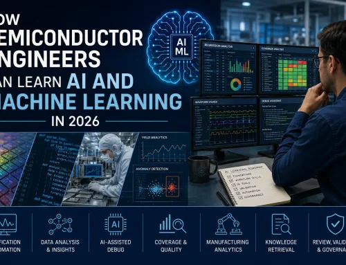
Quick answer: Why is Hanmi Semiconductor trending in 2026?
Hanmi Semiconductor is trending in 2026 because it sits near one of the most important bottlenecks in the AI chip supply chain: advanced packaging for high-bandwidth memory (HBM). The company is not trending simply because AI chips are in demand. It is trending because HBM production depends on specialised packaging equipment, including thermocompression bonders, or TC bonders, and Hanmi is strongly associated with that equipment segment [1], [2].
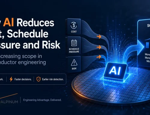
The wider context is clear. AI infrastructure demand is increasing pressure on leading-edge logic, memory, test and packaging capacity. SEMI expects global semiconductor manufacturing equipment sales to reach $145 billion in 2026 and $156 billion in 2027, driven primarily by AI-related investment in leading-edge logic, memory and advanced packaging [1].
For readers asking why Hanmi Semiconductor is suddenly appearing in AI chip, HBM and semiconductor equipment discussions, the answer is therefore not a single news event. It is a combination of AI memory demand, HBM packaging complexity, TC bonder market share, U.S. expansion plans and wider interest in the equipment companies that enable AI chip manufacturing.
What is Hanmi Semiconductor?
Hanmi Semiconductor is a South Korean semiconductor equipment company. It is not the same as Hanmi Pharmaceutical or Hanmi Bank, which can sometimes cause search results to be confused. In the semiconductor context, Hanmi refers to a company that supplies back-end semiconductor manufacturing and packaging equipment.
According to its SEMICON Taiwan 2026 exhibitor profile, Hanmi Semiconductor was founded in 1980 and serves around 340 customers worldwide. The same profile states that the company holds the No. 1 global market share in the TC BONDER market for HBM and has also held the No. 1 global position in micro SAW and Vision Placement, both back-end semiconductor equipment categories [2].
This matters because AI chip demand is not just a front-end wafer-fabrication story. Advanced AI systems need processors, memory, substrates, interposers, packaging, test, assembly and thermal management. As AI hardware becomes more complex, companies supplying specialised packaging and back-end equipment become more strategically visible.
Why Hanmi Semiconductor is trending in 2026
Hanmi Semiconductor is trending because several industry forces are converging simultaneously.
| Reason Hanmi is trending | Why it matters |
| AI chip demand is increasing, and HBM demand | AI accelerators require high memory bandwidth, making HBM supply and packaging capacity strategically important. |
| HBM production needs specialised bonding equipment | TC bonders are used in the HBM manufacturing process to bond memory chips under high temperature and pressure. |
| Hanmi is strongly positioned in TC bonders for HBM | Reports based on TechInsights data place Hanmi first in the HBM TC bonder market with a 71.2% share in 2025. |
| The company is expanding its U.S. presence | Hanmi announced plans to establish Hanmi USA in San Jose by the end of 2026 to support U.S. semiconductor customers. |
| Advanced packaging is becoming a key AI infrastructure bottleneck | AI chips increasingly depend on back-end technologies such as HBM integration, 2.5D packaging, TC bonding and hybrid bonding. |
| Equipment spending is rising | SEMI expects equipment sales to reach record levels by 2027, with AI, memory and advanced packaging as key drivers. |
Reports citing TechInsights data placed Hanmi first in the global HBM TC bonder market in 2025, with cumulative sales of $247.7 million and a 71.2% market share by the third quarter of 2025 [3]. The same reporting identifies TC bonders as key equipment in the HBM process because they bond memory chips under high temperature and pressure [3].
That is the core reason this keyword is appearing. Hanmi is being pulled into search visibility because AI chips are no longer only about GPUs or leading-edge logic. They are also about memory bandwidth, packaging yield, production throughput and equipment availability.
Why HBM matters for AI chips
High-bandwidth memory matters because AI workloads require fast movement of large volumes of data between compute engines and memory. In large AI accelerators, memory bandwidth can become a limiting factor. This is why HBM has become central to the AI hardware discussion.
Reuters reported that SK Hynix recorded a major profit increase as AI demand lifted memory chip demand, with HBM sales more than doubling in 2025. The same report said SK Hynix held a 61% share of the HBM market, according to Macquarie Equity Research [4].
This HBM demand affects the equipment supply chain. More HBM capacity requires more investment in specialised memory production and packaging equipment. SEMI’s equipment forecast specifically links growth to AI-related investments in memory and advanced packaging [1].
For that reason, Hanmi is not trending as an isolated company story. It is trending as part of a wider AI memory infrastructure story.
What is a TC bonder?
A TC bonder is a thermocompression bonding tool used in advanced semiconductor packaging. In simple terms, it helps bond semiconductor dies or memory layers using controlled heat and pressure. In HBM manufacturing, this process is important because multiple memory dies must be stacked and connected with high precision.
The reason TC bonders matter is that HBM is not a simple memory package. It involves stacked memory dies, vertical interconnects and packaging requirements that must support high bandwidth, acceptable thermal behaviour and production yield. As the number of HBM layers increases, bonding accuracy, throughput and process control become more important.
Reports describe the TC bonder as key equipment in the HBM manufacturing process and state that Hanmi entered the HBM market in 2017 with its TSV Dual Stacking TC Bonder [3].
For engineers, the important point is that AI chip performance depends on far more than model architecture or accelerator design. It depends on the physical ability to assemble high-performance memory and logic systems at scale.
Why advanced packaging has become strategic
Advanced packaging has become strategic because AI chips increasingly push against limits in power, bandwidth, interconnect density, thermal behaviour and package-level integration. Instead of relying only on monolithic scaling, AI hardware roadmaps increasingly depend on chiplets, HBM, 2.5D integration, interposers, substrates, bonding and test.
SEMI states that equipment growth is being supported by investment related to AI, especially leading-edge logic, memory and advanced packaging technologies [1]. This is important because back-end assembly, packaging and test are no longer secondary concerns in high-performance AI hardware. They increasingly shape performance, yield, availability, and supply chain resilience.
This is why Hanmi’s role is important. It operates in the part of the supply chain where AI chip demand becomes a manufacturing reality. If HBM and advanced packaging capacity become constrained, equipment suppliers that support those processes become more visible.
Why Hanmi’s U.S. expansion matters
Hanmi is also trending because of its U.S. expansion plan. Manufacturing Dive reported that Hanmi Semiconductor plans to establish Hanmi USA in San Jose, California, by the end of 2026. The facility is expected to act as an integrated operational hub and provide technical support for semiconductor fabs in the United States [5].
This matters for two reasons.
First, semiconductor manufacturing is becoming more regionalised. The U.S. is investing heavily in domestic semiconductor capacity, and advanced packaging is a key part of that strategy. Equipment suppliers need local support capability because production tools require installation, process tuning, maintenance and rapid engineering response.
Second, Hanmi’s U.S. move connects the company more directly with the AI infrastructure ecosystem. Manufacturing Dive reported that the U.S. expansion is linked to rising demand for AI semiconductors and local technical support requirements [5].
For semiconductor leaders, this signals that packaging equipment support is becoming more geographically important. It is not enough to sell equipment globally. Suppliers also need field engineering, service capability and customer proximity in regions where AI semiconductor production is expanding.
TC bonding, wide TC bonders and hybrid bonding
Hanmi’s visibility also reflects interest in what comes after current-generation HBM packaging. As HBM stacks become taller and AI packages become more complex, the industry is exploring ways to improve bonding density, yield, throughput and package performance.
Semiconductor Digest reported that Hanmi planned to launch a second-generation hybrid bonder by the end of 2026 and, before that, a wide TC bonder in the second half of 2026 [6]. This matters because bonding is becoming a technical pressure point in AI hardware manufacturing.
Current TC bonding remains important for HBM, while hybrid bonding is attracting attention for future advanced packaging requirements. The industry needs packaging approaches that can support greater bandwidth, tighter pitches, higher stack counts, and reliable, high-volume production.
What semiconductor teams should watch next
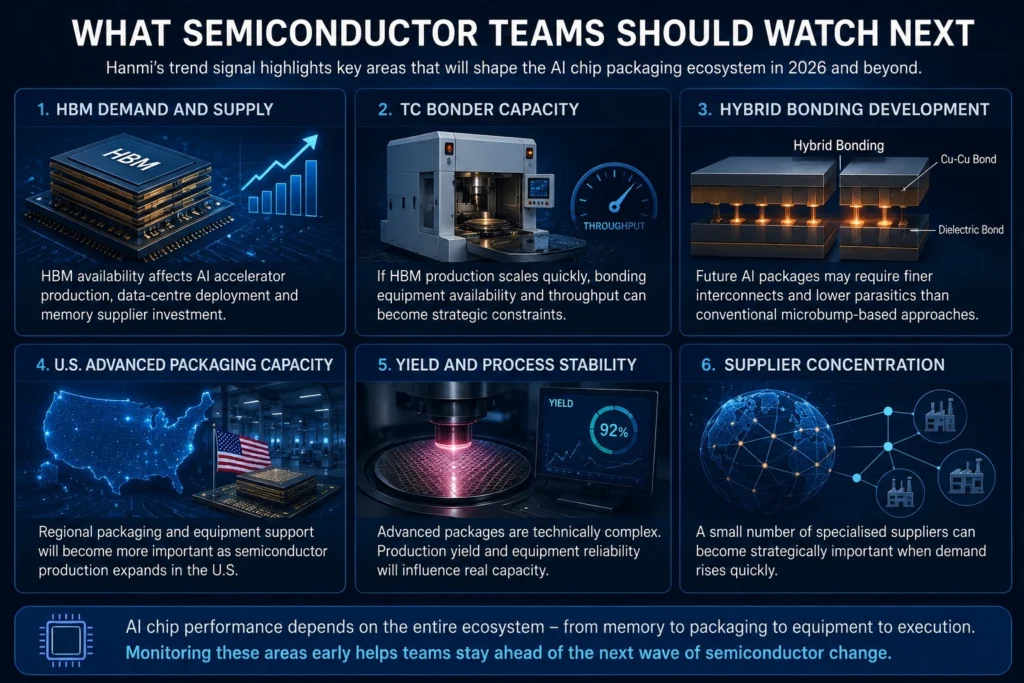
Hanmi’s trend signal should not be viewed only through the lens of one company. It also highlights several broader areas that semiconductor teams should monitor.
| What to watch | Why it matters |
| HBM demand and supply | HBM availability affects AI accelerator production, data-centre deployment and memory supplier investment. |
| TC bonder capacity | If HBM production scales quickly, the availability and throughput of bonding equipment can become strategic constraints. |
| Hybrid bonding development | Future AI packages may require finer interconnects and lower parasitics than conventional microbump-based approaches can support. |
| U.S. advanced packaging capacity | Regional packaging and equipment support will become more important as semiconductor production expands in the U.S. |
| Yield and process stability | Advanced packages are technically complex. Production yield and equipment reliability will influence real capacity. |
| Supplier concentration | A small number of specialised suppliers can become strategically important when demand rises quickly. |
For engineering teams, the key lesson is that AI hardware success depends on the whole manufacturing system. Design, verification, memory, packaging, testing, and supply chain execution all matter. A bottleneck in one part of the chain can affect product availability, schedule confidence and commercial delivery.
This also connects to the wider question of how AI is reshaping semiconductor engineering roles. AI demand is not reducing the importance of semiconductor engineering. There is increasing pressure on engineering teams to manage complexity across design, verification and manufacturing.
Does Hanmi trending mean it is an investment signal?
Not necessarily. This article is an industry and engineering analysis, not investment advice.
A company can trend because it is exposed to a strategically important part of the supply chain. That does not automatically mean its valuation, revenue growth, competitive position or future order book will move in a straight line. Semiconductor equipment markets can be cyclical, customer concentration can be significant, and technology transitions can change supplier dynamics.
The stronger conclusion is more specific: Hanmi Semiconductor is worth watching because HBM, TC bonding, hybrid bonding, and advanced packaging are becoming increasingly important in AI chip manufacturing. That is an industry signal. Any financial conclusion would require separate analysis of valuation, orders, margins, customer concentration, competition and execution risk.
Alpinum perspective: why this matters for AI and semiconductor engineering
Hanmi Semiconductor’s visibility is another example of a larger shift in the semiconductor industry. AI demand is increasing attention on parts of the supply chain that were previously less visible to non-specialist readers. The discussion is no longer only about who designs the AI accelerator. It is also about who can reliably verify, manufacture, package, test, and scale it.
For engineering leaders, this reinforces three points.
First, AI hardware depends on semiconductor execution across many domains. Chip design, design verification capability, memory integration, packaging, test and manufacturing all affect the final product.
Second, advanced packaging is now a strategic technology area. HBM, chiplets, and 2.5D integration create new dependencies among design choices, manufacturing capabilities, and supply-chain resilience.
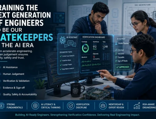
Third, AI does not reduce the need for semiconductor engineers. It raises the bar. Engineers are needed to manage system-level trade-offs, verification confidence, manufacturing constraints and production risk. This is why structured AI adoption in design verification must remain connected to governance, review quality and measurable engineering outcomes.
For teams managing complex projects, this also links to system-scale programme risk in verification. AI hardware programmes depend on confidence across architecture, implementation, verification, manufacturing, and supply chain execution.
Conclusion: Why Hanmi Semiconductor is trending in 2026
Hanmi Semiconductor is trending in 2026 because demand for AI chips has made HBM and advanced packaging strategically important. HBM production depends on specialised equipment, and TC bonders are part of that manufacturing path. Hanmi’s position in TC bonders for HBM, its reported market share, its U.S. expansion plan, and its next-generation bonding roadmap all place it near one of the key pressure points in the AI semiconductor supply chain [2], [3], [5], [6].
The broader lesson goes beyond Hanmi. AI infrastructure depends on more than GPUs and model training. It depends on memory bandwidth, packaging capacity, process control, test capability, equipment availability and regional manufacturing support.
For semiconductor leaders, the main takeaway is that AI is not only changing software and data-centre economics. It is changing the visibility of semiconductor manufacturing equipment, advanced packaging and the engineering teams responsible for turning AI chip demand into reliable production capacity.
Semiconductor AI Success Depends on Engineering Execution
AI infrastructure demand is increasing attention to advanced packaging, verification capabilities, manufacturing scalability, and system-level engineering confidence. For semiconductor teams, the challenge is no longer only building AI hardware. It ensures reliable execution across design, verification, and production workflows.
Explore related Alpinum insights:
- “AI in DV” adoption and workflow capability
https://alpinumconsulting.com/services/ai-in-dv/adoption/ - Semiconductor verification expertise
https://alpinumconsulting.com/services/designverification/
- Formal verification and sign-off confidence
https://alpinumconsulting.com/blogs/verification/growing-role-formal-verification-risc-v-design/
FAQs:Why Is Hanmi Semiconductor Trending in 2026?
Hanmi Semiconductor is trending because AI chip demand is drawing increased attention to HBM, TC bonders, advanced packaging, and semiconductor equipment capacity.
Hanmi Semiconductor is a South Korean semiconductor equipment company. It supplies back-end semiconductor manufacturing and packaging equipment, including TC bonders for HBM.
No. Hanmi Semiconductor is not a chip designer or memory chip producer. It is a semiconductor equipment supplier focused on manufacturing and packaging equipment.
A TC bonder, or thermocompression bonder, is a piece of equipment used in advanced semiconductor packaging. In HBM manufacturing, it helps bond stacked memory chips using controlled heat and pressure.
HBM matters because AI accelerators need high memory bandwidth to move large amounts of data quickly. This makes HBM supply and packaging capacity important for AI infrastructure.
Hanmi is linked to HBM because it supplies TC bonders used in HBM manufacturing. Reports based on TechInsights data placed Hanmi first in the HBM TC bonder market in 2025.
Hanmi’s planned San Jose subsidiary matters because semiconductor companies need local equipment support, field engineering and technical service as U.S. AI semiconductor manufacturing capacity expands.
TC bonding uses heat and pressure to bond semiconductor components. Hybrid bonding is a more advanced packaging approach that can support finer interconnects and is being watched for future high-performance chip packaging.
Not necessarily. Hanmi’s trend signal reflects industry interest in HBM and packaging equipment. Investment decisions require separate analysis of valuation, orders, margins, competition and risk.
References
[1] SEMI, “Global Semiconductor Equipment Sales Projected to Reach a Record of $156 Billion in 2027,” Dec. 2025. [Online]. Availablehttps://www.semi.org/en/semi-press-release/global-semiconductor-equipment-sales-projected-to-reach-a-record-of-156-billion-dollars-in-2027-semi-reports
[2] SEMICON Taiwan 2026, “HANMI Semiconductor Exhibitor Profile.” [Online]. Available: https://expo.semi.org/taiwan2026/Public/eBooth.aspx?BoothID=652381.
[3] Maeil Business Newspaper, “HANMI Semiconductor Achieves 71% Global Market Share,” Dec. 2025. [Online]. Available: https://www.mk.co.kr/en/business/11504116.
[4] Reuters, “SK Hynix posts forecast-beating Q4 profit on huge AI demand,” Jan. 2026. [Online]. Available: https://www.reuters.com/world/asia-pacific/sk-hynix-posts-forecast-beating-q4-profit-huge-ai-demand-2026-01-28/.[5] Manufacturing Dive, “Hanmi Semiconductor to enter US market with California subsidiary,” May 2026. [Online]. Available: https://www.manufacturingdive.com/news/hanmi-semiconductor-expand-san-jose-subsidiary-artificial-intelligence/820763/.

Written by : Mike Bartley
Mike started in software testing in 1988 after completing a PhD in Math, moving to semiconductor Design Verification (DV) in 1994, verifying designs (on Silicon and FPGA) going into commercial and safety-related sectors such as mobile phones, automotive, comms, cloud/data servers, and Artificial Intelligence. Mike built and managed state-of-the-art DV teams inside several companies, specialising in CPU verification.
Mike founded and grew a DV services company to 450+ engineers globally, successfully delivering services and solutions to over 50+ clients.
Mike started Alpinum in April 2016 to deliver a range of start-of-the art industry solutions:
Alpinum AI provides tools and automations using Artificial Intelligence to help companies reduce development costs (by up to 90%!) Alpinum Services provides RTL to GDS VLSI services from nearshore and offshore centres in Vietnam, India, Egypt, Eastern Europe, Mexico and Costa Rica. Alpinum Consulting also provides strategic board level consultancy services, helping companies to grow. Alpinum training department provides self-paced, fully online training in System Verilog, UVM Introduction and Advanced, Formal Verification, DV methodologies for SV, UVM, VHDL and OSVVM and CPU/RISC-V. Alpinum Events organises a number of free-to-attend industry events
You can contact Mike (mike@alpinumconsulting.com or +44 7796 307958) or book a meeting with Mike using Calendly (https://calendly.com/mike-alpinum-consulting).
Stay Informed and Stay Ahead
Latest Articles, Guides and News
Explore related insights from Alpinum that dive deeper into design verification challenges, practical solutions, and expert perspectives from across the global engineering landscape.