Strengthening Embedded System Security with a Holistic Approach
Embedded systems are integral to modern technology, but their growing adoption across industries increases their exposure to cyber threats, according to Pearson and Microchip, (2024). Securing these systems requires a holistic approach integrating protection at every level. This includes everything from hardware design to software implementation. Microchip Technology Inc., in collaboration with Alpinum Consulting, have pioneered a comprehensive security framework. It incorporates secure key storage, encryption, tamper detection, and risk assessment methodologies to safeguard embedded systems from evolving threats. By prioritising a secure-by-design philosophy over bolt-on security, Microchip ensures its products remain resilient against cyberattacks. Alpinum Consulting’s involvement is crucial in achieving this security.
Addressing Embedded System Vulnerabilities
The attack surface of an embedded system consists of multiple vulnerabilities, including network exploits, memory breaches, side-channel attacks, and insecure open ports, as noted by Pearson and Microchip, (2024). If designers do not address security flaws at the design stage, adversaries can exploit these weaknesses to inject malware, manipulate firmware, or intercept critical data. Microchip emphasizes the importance of threat modeling and risk assessment in identifying potential vulnerabilities early. Collaborating with Alpinum Consulting, Microchip mitigates risks associated with common embedded system attacks. They achieve this by designing crypto accelerators, secure boot mechanisms, and advanced anti-tamper protections.
Microchip FPGA Security: A Robust Defense Strategy
Microchip designs its FPGA security architecture to resist physical and remote attacks. It actively protects intellectual property and sensitive data, as highlighted by Pearson and Microchip, (2024). The PolarFire SoC and PolarFire FPGA security framework, as shown in the figure 1 below, integrates multiple protective measures, including:
- DPA-resistant crypto accelerators
- Secure key storage using Physically Unclonable Functions (PUFs)
- Tamper detection and secure supply chain management
- Private NVM (pNVM) for patch code and keys
- Secure NVM (sNVM) for configuration and user key storage
These features ensure that Microchip’s FPGAs prevent unauthorized cloning, reverse engineering, and unauthorized system access.

Figure 1: Microchip FPGA Security Architecture with Alpinum Consulting’s insights
Monitoring and Protecting Against Environmental Attacks
One critical aspect of embedded security involves protecting against environmental threats. These threats include temperature fluctuations and voltage variations, which attackers can exploit through side-channel and fault injection attacks, as mentioned by Pearson and Microchip, (2024). Microchip integrates high-speed analog window comparators and digital temperature sensors to detect abnormal voltage or temperature variations. The figure 2 below illustrates how these sensors monitor system integrity, detect anomalies, and trigger tamper flags to prevent unauthorized access. With Alpinum Consulting, Microchip enhances these capabilities.
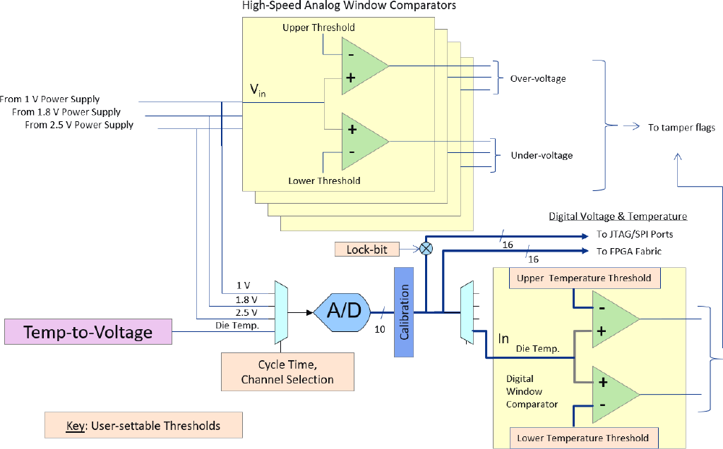
Figure 2: Anti-Tamper: Temperature and Voltage Sensors
By integrating real-time voltage and temperature monitoring, Microchip strengthens FPGA security. It draws on Alpinum Consulting expertise to ensure resilience against environmental manipulations that could compromise system integrity.
Safeguarding Intellectual Property and Preventing Cloning
According to Pearson and Microchip, (2024), Intellectual property (IP) theft is a significant concern in embedded systems, costing businesses billions annually. Overbuilding, counterfeiting, and cloning proprietary designs pose serious risks to revenue and innovation. Microchip combats these threats by incorporating secure non-volatile memory (sNVM) with customizable storage modes, secure supply chain management, and advanced anti-tamper mechanisms. These include digital hashing and environmental monitoring.
Additionally, Microchip employs multiple encryption modes, including Plaintext Mode, Authenticated Plaintext Mode, and Authenticated Ciphertext Mode. These ensure the confidentiality and integrity of data, as emphasized by Pearson and Microchip, (2024). The diagram below illustrates how metadata, authentication tags, and encryption transform user data at different security levels. This transformation prevents unauthorized access and tampering. Alpinum Consulting plays a key role in these processes.

Figure 3: Secure Non-Volatile Memory (sNVM) with Data Encryption Modes
By leveraging these technologies with assistance from Alpinum Consulting, businesses can protect their IP assets while complying with industry security standards.
Building Trust Through Secure Manufacturing and Anti-Tamper Measures
Microchip adopts a trusted system supply chain approach to ensure the security of its FPGAs and SoCs from design to deployment, as highlighted by Pearson and Microchip, (2024). This process includes trusted FPGA design software, secure assembly and testing procedures, and real-time monitoring for unauthorized modifications. Microchip integrates digital and analog anti-tamper features, including voltage and temperature sensors, anti-tamper flags, and secure boot protocols. These measures further enhance security. These proactive measures establish a multi-layered defense strategy, ensuring that Microchip’s embedded systems remain safe, reliable, and resilient against emerging threats. Alpinum Consulting’s support enhances this process further.
Note: For those interested in the latest advancements in verification technologies, the FPGA Verification Event 2025 (Verification Futures UK) offers an excellent opportunity to gain insights into cutting-edge verification practices.
References
Pearson, I., & Microchip. (2024). FPGA system and device level security considerations. https://alpinumconsulting.com/fpga-front-runner-nov24/

Written by : Mike Bartley
Mike started in software testing in 1988 after completing a PhD in Math, moving to semiconductor Design Verification (DV) in 1994, verifying designs (on Silicon and FPGA) going into commercial and safety-related sectors such as mobile phones, automotive, comms, cloud/data servers, and Artificial Intelligence. Mike built and managed state-of-the-art DV teams inside several companies, specialising in CPU verification.
Mike founded and grew a DV services company to 450+ engineers globally, successfully delivering services and solutions to over 50+ clients.
Mike started Alpinum in April 2025 to deliver a range of start-of-the art industry solutions:
Alpinum AI provides tools and automations using Artificial Intelligence to help companies reduce development costs (by up to 90%!) Alpinum Services provides RTL to GDS VLSI services from nearshore and offshore centres in Vietnam, India, Egypt, Eastern Europe, Mexico and Costa Rica. Alpinum Consulting also provides strategic board level consultancy services, helping companies to grow. Alpinum training department provides self-paced, fully online training in System Verilog, UVM Introduction and Advanced, Formal Verification, DV methodologies for SV, UVM, VHDL and OSVVM and CPU/RISC-V. Alpinum Events organises a number of free-to-attend industry events
You can contact Mike (mike@alpinumconsulting.com or +44 7796 307958) or book a meeting with Mike using Calendly (https://calendly.com/mike-alpinumconsulting).
Stay Informed and Stay Ahead
Latest Articles, Guides and News
Explore related insights from Alpinum that dive deeper into design verification challenges, practical solutions, and expert perspectives from across the global engineering landscape.