At ISSCC 2026, Session 29 on biochemical sensors for life sciences and agriculture included a paper that stood out for a simple reason: it addressed the real scaling problem in solid-state nanopore sensing at the circuit and system level, not just at the single-channel level. In “A 256-Channel Event-Driven Readout for Solid-State Nanopore Single-Molecule Sensing with 193 pArms Noise in a 1 MHz Bandwidth,” researchers from KU Leuven and imec presented a complete front-end architecture that combines low-noise current sensing, event detection, and shared sampling resources to improve power, area, and data efficiency together [1].
For readers interested in how mixed-signal design choices shape the future of life-science instrumentation, this paper is particularly relevant. It shows that the challenge in nanopore sensing is no longer only whether a single pore can be read accurately. The more important question is whether hundreds of pores can be monitored with the bandwidth, sensitivity, and efficiency needed for practical high-throughput systems. That is the problem this work sets out to solve.
| Key learning point | Link to detailed explanation | External reference |
| Scaling nanopore sensing is limited by power, area, and data rate, not just sensing accuracy. | The scaling problem is power, area, and data rate | [1], [3] |
| Event-driven architectures improve efficiency by processing only meaningful molecular activity instead of continuous data streams. | Why event-driven detection matters | [1] |
| System-level design, including dynamic resource allocation, is critical for reducing data bottlenecks in multi-channel sensing. | A 256-channel readout designed for scalable sensing | [1] |
| Measured performance must balance bandwidth, noise, and per-channel efficiency to enable practical deployment. | Measured performance | [1], [5] |
| Real-world validation using biological experiments is essential to prove that circuit innovations translate into usable sensing systems. | Biological validation under real sensing conditions | [1], [4], [7] |
Why nanopore sensing matters
Nanopore sensing identifies single molecules by measuring changes in ionic current as molecules pass through a nanoscale pore. When a molecule such as DNA translocates through the pore, it partially blocks ion flow and induces a measurable modulation of the current. The amplitude and duration of that signal can then be used to infer molecular characteristics. This makes nanopore sensing attractive for applications such as DNA analysis, protein detection, molecular diagnostics, and other high-resolution biochemical measurements.
Solid-state nanopores are especially interesting because they are robust, compatible with semiconductor manufacturing, and capable of producing larger signal amplitudes than biological nanopores. In principle, that creates a path to faster per-pore readout and potentially lower-cost, more scalable sensing platforms. In practice, however, the electronics quickly become the bottleneck. The front-end must maintain low noise at MHz-class bandwidth while operating under realistic nanopore currents and input capacitances. That combination places heavy demands on the readout architecture.
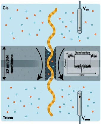
Figure 1. DNA translocation through a solid-state nanopore produces measurable current dips that carry molecular information [1].
Figure 1 helps ground the discussion in the basic sensing mechanism. The paper uses this context to show why solid-state nanopores are promising, while also making clear that signal quality depends as much on the readout electronics as on the pore itself.
The scaling problem is power, area, and data rate
The paper frames the core challenge clearly. Existing integrated readouts for solid-state nanopores are difficult to scale because low-noise sensing typically requires excessive power and silicon area per pore. At the same time, larger pore arrays generate very high data rates, especially when high temporal resolution is needed. The result is that many prior approaches can support only a few dozen pores while maintaining an acceptable signal-to-noise ratio, leaving the throughput of solid-state nanopores well below that of large biological nanopore arrays.
This is what makes the ISSCC 2026 paper significant. It does not treat noise, area, power, and throughput as separate problems. Instead, it addresses them as linked system constraints. That is an important architectural mindset for any sensing platform that needs to move from interesting laboratory demonstrations to practical multi-channel deployment.
A 256-channel readout designed for scalable sensing
The proposed chip implements a complete 256-channel front end for event-driven single-molecule sensing using solid-state nanopores in 65 nm CMOS. Its central innovation is a new integrate-and-hold transimpedance amplifier combined with per-channel event detection. Rather than continuously digitising every channel at full rate, the architecture monitors each pore and routes data forward only when a relevant event is detected.
At the channel level, the design uses an integration capacitor, reset switch, output buffer, and input stage arranged to reduce noise while keeping the required bandwidth. The architecture also leverages the nanopore’s high output resistance and employs bandwidth-limiting techniques to improve consistency across varying nanopore characteristics and signal levels. The paper’s technical contribution is therefore not just that it senses current, but that it does so with a structure intended from the start for array-level scaling.
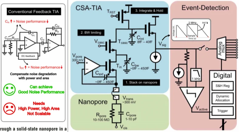
Figure 2. The proposed readout channel combines a charge-sensitive TIA with event detection and a first-order nanopore model to improve per-pore efficiency [1].
Figure 2 is the key architecture image in the paper. It shows that the design is not simply a better low-noise front end, but a coordinated sensing chain in which analogue readout and event-driven control work together to improve scalability.
Why event-driven detection matters
One of the strongest ideas in the paper is the use of time sparsity. Molecular translocation events do not happen continuously, so most pores are idle most of the time. The chip exploits that by integrating an event-detection circuit on each channel. Only data from active pores is forwarded to the ADC path, which reduces the amount of data the system needs to process and transmit. According to the paper, this reduces the overall ADC data rate by 32×.
The system architecture includes 256 TIAs, eight sample-and-hold slots, and a 12-bit pipelined SAR ADC operating at 16 MHz. Any active pore can dynamically connect to an available sample-and-hold slot. Compared with static allocation, this dynamic approach reduces the number of missed events for the same slot count. The authors report that eight slots provide a good trade-off, limiting data loss to around 0.1% while also lowering area, power, and downstream processing burden.
For engineering teams, that is the paper’s broader lesson. The real efficiency gain does not come from analogue performance alone. It comes from treating sensing activity as sparse and designing the readout chain accordingly. That is an architecture-level decision with direct consequences for throughput and deployment cost.
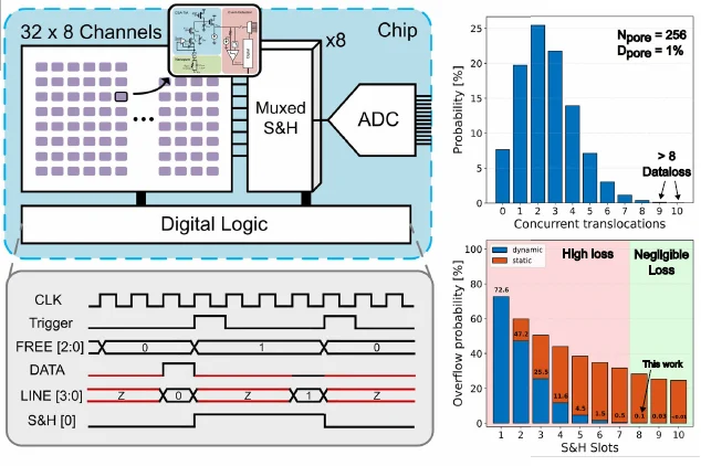
Figure 3. Dynamic allocation lets active nanopores claim shared sampling resources, reducing missed events and lowering the data burden on the conversion path [1].
Figure 3 illustrates why this design is best understood as a system solution rather than a front-end-only improvement. The timing and allocation scheme are central to the paper’s 32× data-rate reduction claim and to its overall scaling argument.
Measured performance
The measured results are strong enough to justify the attention this paper has received. For a typical 10 nA nanopore baseline current and 7.1 pF input capacitance, the TIA achieves 193 pArms input-referred noise over a 1 MHz bandwidth. The full-system noise rises to 258 pArms due to noise folding from an overdesigned ADC driver, which the authors note could be further improved with driver optimisation. The gain-boosting op-amp extends the TIA bandwidth from 200 kHz to 1 MHz, helping the design meet the temporal requirements of fast nanopore events.
Equally important are the per-pore efficiency numbers. The chip achieves 1 mW of power per pore and 0.019 mm² of area per pore, while reducing the total data rate to 288 Mbit/s. Those are the numbers that move the discussion beyond elegant circuitry and into the question of how a readout can support meaningful channel-count scaling.
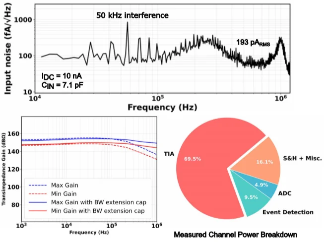
Figure 4. Measured noise, transfer characteristics, and channel power breakdown show how the design balances bandwidth, sensitivity, and efficiency [1].
Figure 4 is useful because it turns the headline numbers into engineering evidence. It shows the measured noise behaviour, transfer response across gain settings, and where channel power is consumed, which together support the paper’s claim of improved per-pore scalability.
Biological validation under real sensing conditions
The work becomes even more compelling because it was not evaluated only as an electrical prototype. The authors also tested the chip biologically using SiN solid-state nanopores with diameters ranging from 10 to 30 nm. Measurements were performed in 4 M LiCl, buffered to pH 8.0, using Ag/AgCl electrodes. DNA molecules were modified using a DNA-origami protocol to include three 17-dumbbell labels, then driven through the pore using a 200 mV cross-membrane bias.
These experiments produced current dips of approximately 0.5 nA, and the expected molecular signature with three distinct spikes was visible in the translocation traces. That matters because it shows the readout can do more than post attractive bench metrics. It can resolve biologically relevant labelled DNA events in a way that supports the paper’s case for practical single-molecule sensing.
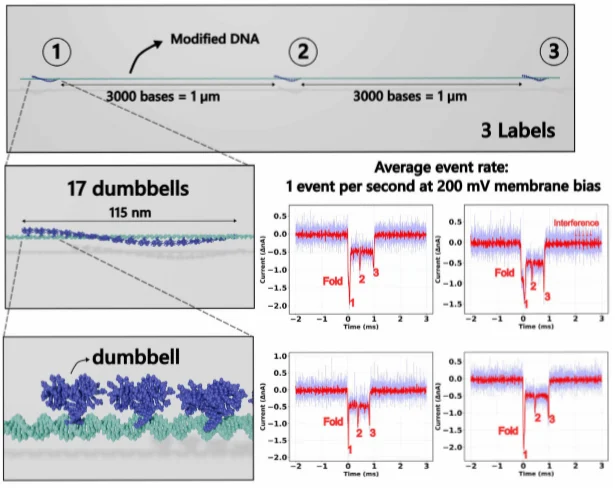
Figure 5. Labelled DNA translocation traces show that the readout can capture distinct molecular signatures under realistic nanopore test conditions [1].
Figure 5 is one of the most important visuals in the paper because it links circuit architecture to sensing outcome. It shows that the system is not only efficient on paper, but also capable of resolving the event structure needed for real molecular detection.
How it compares with prior nanopore readouts
The authors benchmark the system against prior nanopore readout work and position it as the first 256-channel solid-state nanopore interface with significantly improved power and area efficiency per pore. In the comparison presented in the paper, this design achieves the highest channel count, the smallest area per channel, and the lowest power per channel, while maintaining competitive noise performance and integrating on-chip event detection. The conclusion states that the architecture delivers a 10× improvement in scalability compared with earlier solid-state nanopore readout interfaces.
That comparison should be interpreted carefully, as always, because bandwidth, load assumptions, and measurement conditions vary across publications. Even so, the architectural significance is clear. This work shows a practical route to scaling solid-state nanopore electronics without abandoning the bandwidth and sensitivity requirements that make single-molecule sensing useful in the first place.
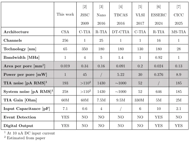
Figure 6. The paper’s benchmark comparison highlights the combination of high channel count, low per-pore area, low per-pore power, and integrated event detection [1].
Figure 6 helps readers see why this ISSCC paper is notable. The value is not a single best-in-class number in isolation, but rather the way several important metrics improve together to support real scaling.
What this means for life-science instrumentation
From a life-science perspective, the importance of this work lies in throughput, cost, and practicality. If solid-state nanopore systems are to support broader use in diagnostics, assay development, or future point-of-care tools, the readout electronics must scale without imposing a disproportionate penalty in power, die area, or data movement for each additional pore. That is precisely the issue this design addresses. The authors explicitly connect the resulting increase in molecular throughput with the potential to shorten diagnostic lead times and lower costs in future applications.
For semiconductor engineers, the paper also offers a broader lesson. In sensor interfaces, architecture decisions around bandwidth allocation, event detection, and shared resources reflect broader system-level design and verification approaches that determine whether complex systems can scale effectively. A scalable sensing platform is rarely the result of one better amplifier. More often, it emerges from a coordinated design strategy that aligns front-end performance, data handling, and system utilisation. This ISSCC 2026 paper is a strong example of that principle.
Conclusion
The ISSCC 2026 nanopore readout paper from KU Leuven and imec is important because it tackles a real deployment problem with a real system answer. By combining a new integrate-and-hold TIA, per-channel event detection, dynamic sample allocation, and biologically validated operation, the design moves solid-state nanopore sensing closer to practical high-throughput use. It is a useful reminder that in biochemical sensing, better system architecture is often what turns an interesting measurement concept into a scalable instrument platform.
References
[1] S. Crols, C. Mora Lopez, F. Tavernier, M. Verhelst, and N. Van Helleputte,“A 256-Channel Event-Driven Readout for Solid-State Nanopore Single-Molecule Sensing with 193 pArms Noise in a 1 MHz Bandwidth,” in Proc. IEEE Int. Solid-State Circuits Conf. (ISSCC), 2026, doi: 10.1109/ISSCC49663.2026.11409180. [2] M. Jain et al., “Nanopore sequencing and assembly of a human genome with ultra-long reads,” Nature Biotechnology, vol. 36, no. 4, pp. 338–345, 2018, doi: 10.1038/nbt.4060. [3] Q. Lin et al., “Advances and challenges in integrated circuits for electrochemical sensing: Enabling next-generation biomedical and molecular applications,” IEEE Trans. Biomed. Circuits Syst., pp. 1–21, 2025, doi: 10.1109/TBCAS.2025.3589027. [4] C.-C. Chien et al., “Single-stranded DNA translocation recordings through solid-state nanopores on glass chips at 10 MHz measurement bandwidth,” ACS Nano, vol. 13, no. 9, pp. 10545–10554, 2019, doi: 10.1021/acsnano.9b04626. [5] M. Crescentini, M. Bennati, M. Carminati, and M. Tartagni, “Noise limits of CMOS current interfaces for biosensors: A review,” IEEE Trans. Biomed. Circuits Syst., vol. 8, no. 2, pp. 278–292, 2014, doi: 10.1109/TBCAS.2013.2262998. [6] J. K. Rosenstein and K. L. Shepard, “Temporal resolution of nanopore sensor recordings,”
in Proc. IEEE Eng. Med. Biol. Soc. (EMBC), 2013, pp. 4110–4113, doi: 10.1109/EMBC.2013.6610449. [7] N. A. W. Bell and U. F. Keyser, “Digitally encoded DNA nanostructures for multiplexed, single-molecule protein sensing with nanopores,” Nature Nanotechnology, vol. 11, no. 7, pp. 645–651, 2016, doi: 10.1038/nnano.2016.50.
Explore related engineering insights and approaches
For engineers working on scalable sensing systems, mixed-signal architectures, and system-level optimisation, the following resources provide deeper perspectives:
- System-level verification in complex architectures
- Risk-based verification: focusing effort where it matters most
- Verification capability benchmarking and engineering maturity
- Scaling FPGA-based systems and compute architectures
- Embedded software design and system integration considerations
Explore training and engineering support
If you are developing scalable sensing systems or complex semiconductor architectures, you can explore Alpinum’s training and engineering support:
- Upcoming Semiconductor and Verification Training Programmes
- Embedded Software Testing & Validation Services Support
- FPGA and System Prototyping Services
- Design verification services and system-level engineering support

Written by : Mike Bartley
Mike started in software testing in 1988 after completing a PhD in Math, moving to semiconductor Design Verification (DV) in 1994, verifying designs (on Silicon and FPGA) going into commercial and safety-related sectors such as mobile phones, automotive, comms, cloud/data servers, and Artificial Intelligence. Mike built and managed state-of-the-art DV teams inside several companies, specialising in CPU verification.
Mike founded and grew a DV services company to 450+ engineers globally, successfully delivering services and solutions to over 50+ clients.
Mike started Alpinum in April 2025 to deliver a range of start-of-the art industry solutions:
Alpinum AI provides tools and automations using Artificial Intelligence to help companies reduce development costs (by up to 90%!) Alpinum Services provides RTL to GDS VLSI services from nearshore and offshore centres in Vietnam, India, Egypt, Eastern Europe, Mexico and Costa Rica. Alpinum Consulting also provides strategic board level consultancy services, helping companies to grow. Alpinum training department provides self-paced, fully online training in System Verilog, UVM Introduction and Advanced, Formal Verification, DV methodologies for SV, UVM, VHDL and OSVVM and CPU/RISC-V. Alpinum Events organises a number of free-to-attend industry events
You can contact Mike (mike@alpinumconsulting.com or +44 7796 307958) or book a meeting with Mike using Calendly (https://calendly.com/mike-alpinumconsulting).
Stay Informed and Stay Ahead
Latest Articles, Guides and News
Explore related insights from Alpinum that dive deeper into design verification challenges, practical solutions, and expert perspectives from across the global engineering landscape.