Introduction: Why Quantum Hardware Needs EDA Discipline
Quantum computing hardware has advanced rapidly in laboratory settings, particularly in qubit coherence, control fidelity, and experimental scale. However, the processes used to design and evolve this hardware remain largely experimental. Much of today’s quantum chip development still relies on informal iteration, specialist knowledge, and manual tuning rather than structured engineering flows.
As qubit counts increase and architectures diversify, this approach becomes increasingly fragile. Small parameter changes can alter system behaviour in ways that are difficult to predict, reproduce, or verify. Iteration cycles slow, root causes become harder to isolate, and scaling decisions are often taken with limited confidence.
In classical semiconductor development, Electronic Design Automation (EDA) enabled teams to move from bespoke design to repeatable, system-scale engineering. Quantum EDA seeks to introduce a similar discipline, not by abstracting away the physics, but by making design intent explicit, traceable, and testable as systems grow. Without this transition, progress beyond small quantum demonstrators is likely to remain inconsistent and high-risk.
What Quantum EDA Encompasses
Quantum EDA refers to software frameworks and workflows that support the modelling, simulation, optimisation, and verification of quantum hardware. These tools may incorporate quantum algorithms directly, or may be classical tools purpose-built for quantum-specific devices and constraints.
Unlike classical EDA, where abstraction layers are well established, quantum EDA must bridge multiple domains simultaneously:
- Device physics and material behaviour
- Circuit-level electromagnetic effects
- Cryogenic operation and control constraints
- System-level coherence, coupling, and noise interactions
The challenge is not purely computational. It lies in structuring design knowledge so that assumptions, constraints, and trade-offs are visible and testable across the full hardware stack.
How Quantum EDA Works in Practice
Quantum-Enhanced Optimisation
Specific quantum design problems map naturally to combinatorial optimisation. Layout configuration, coupling optimisation, and frequency allocation can become intractable as system size grows. Quantum-enhanced approaches attempt to explore these design spaces more efficiently by exploiting quantum parallelism.
Rather than evaluating design options sequentially, quantum algorithms can encode multiple candidate solutions simultaneously. In practice, these techniques are applied to tightly scoped sub-problems rather than entire design flows, reflecting current hardware limitations.
Hybrid Quantum–Classical Workflows
Most practical Quantum EDA implementations today are hybrid. Classical solvers manage orchestration, parameter sweeps, and verification checks, while quantum processors or quantum-inspired solvers are applied selectively to optimisation kernels.
Hybrid workflows recognise a practical reality: quantum hardware remains scarce, noisy, and specialised. Classical tools continue to play a central role in validation, integration, and decision-making.
Problem Transformation and QUBO Mapping
To exploit quantum solvers, design problems must be reformulated into representations such as Quadratic Unconstrained Binary Optimisation (QUBO). This translation step is non-trivial. Poor formulations can obscure physical constraints or yield mathematically valid but physically meaningless solutions.
Quantum EDA, therefore, encompasses not only solver execution but also the expertise required to encode constraints correctly and interpret results within an engineering context.
Key Application Areas
Superconducting Qubit Design
Superconducting qubits demand precise control over geometry, materials, and electromagnetic environments. Slight variations can lead to frequency collisions, unintended coupling, or coherence loss.
Quantum EDA tools support:
- Parameterised circuit layout generation
- Electromagnetic simulation for coupling and cross-talk analysis
- Frequency planning and spacing optimisation
- Extraction of effective Hamiltonian parameters
These capabilities allow engineers to reason systematically about design margins rather than relying on trial-and-error prototyping.
Spin Qubit Systems and TCAD
Spin qubits sit at the intersection of semiconductor device physics and quantum behaviour. Here, electrostatic confinement, disorder, and interface quality dominate in determining qubit performance.
At the device level, quantum behaviour emerges directly from geometry and electrostatic potential profiles. Slight variations in gate layout or material interfaces can shift confinement regimes and interaction strengths, with measurable impact on coherence and control.
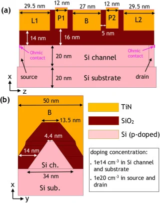
Figure 1: Device-level electrostatic confinement in spin-based quantum hardware. Source: SCIENCEDIRECT
High-resolution simulations showing how gate geometry and electrostatic potential define confinement regimes and influence qubit behaviour.
Figure 1 illustrates how electrostatic confinement and geometry influence quantum behaviour at the device level, motivating the use of high-resolution TCAD within Quantum EDA workflows. By linking physical structure to extracted qubit parameters, these tools enable controlled exploration of design trade-offs rather than manual tuning.
Workflow Automation and Integration
Beyond individual simulations, Quantum EDA addresses the orchestration of complete design flows. These workflows include schematic capture, layout generation, EM analysis, and data management across design iterations.
Automation improves traceability and consistency while enabling collaboration between physicists, device engineers, and system architects using shared artefacts rather than informal documentation.
Example Tools and Platforms
To support the workflows described above, a range of Quantum EDA tools has emerged across different abstraction levels. These tools are not interchangeable and typically address specific aspects of the quantum hardware design stack.
- Qiskit Metal provides an open-source framework for parameterised layout and electromagnetic modelling of superconducting quantum circuits, enabling geometry-driven design exploration.
- QuantumPro (Keysight) integrates superconducting chip design, simulation, and parameter extraction within a unified workflow, supporting iterative refinement of qubit and resonator layouts.
- KQCircuits, built on KLayout, offers a library-based approach to reusable superconducting qubit structures, reflecting early efforts to formalise design reuse in quantum hardware.
- QTCAD® (Nanoacademic) focuses on high-resolution device-level simulation for spin qubits, linking electrostatic confinement and material properties to extracted qubit parameters.
- SpinQ QEDA targets accessibility and rapid iteration, providing a web-based environment for early-stage quantum chip design.
These examples illustrate the diversity of approaches within Quantum EDA. In practice, tool selection depends on qubit technology, required fidelity, system maturity, and the degree of integration needed among device, circuit, and system levels.
System-Level Constraints and Trade-offs
Quantum EDA operates under constraints that differ fundamentally from those encountered in classical digital design. System behaviour is dominated by noise and decoherence rather than deterministic logic margins. Manufacturing variability can have a disproportionate impact on performance and yield. Verification often relies on probabilistic measurements, and design rules continue to evolve alongside hardware architectures.
These constraints are compounded by the fact that quantum hardware is inherently a vertically coupled system. Practical implementations span room-temperature control and measurement electronics, cryogenic signal routing, amplification chains, and quantum devices operating at millikelvin temperatures. Decisions made at one level frequently constrain behaviour at others, sometimes in non-obvious ways.
A simplified system schematic helps clarify how these constraints manifest across a practical cryogenic quantum computing stack. Figure 2 illustrates this coupling, showing why Quantum EDA cannot be confined to qubit layout or circuit simulation alone. Adequate design flows must account for interactions among thermal stages, control placement, signal integrity, and device interfaces to preserve design intent as systems scale.
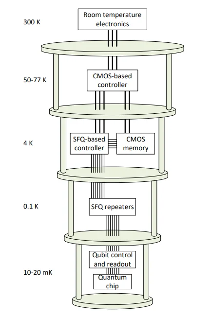
Figure 2: System-level view of a cryogenic quantum computing stack. Source:
Conceptual illustration showing the coupling between room-temperature control electronics, cryogenic signal paths, quantum processing units, and amplification stages.
As a result, increased automation does not automatically translate into increased confidence. Poor abstractions can obscure critical failure modes rather than expose them. Effective Quantum EDA therefore prioritises transparency, traceability, and validation across the full hardware stack, treating optimisation as a controlled outcome rather than a primary objective.
Why Quantum EDA Matters for Scale
The significance of Quantum EDA lies in enabling a transition from experimental success to engineering reliability. As systems grow, informal practices break down. Design intent becomes implicit, assumptions are lost, and debugging becomes retrospective.
By enforcing structure, Quantum EDA helps teams:
- Expose assumptions early
- Quantify design margins explicitly
- Compare architectures systematically
- Reduce iteration cycles without reducing insight
This approach mirrors the historical role of classical EDA, not by copying its abstractions, but by applying its engineering discipline to fundamentally different physics.
Continue Exploring
If you would like to explore more work in this area, see the related articles in the Quantum section on the Alpinum website:
https://alpinumconsulting.com/resources/blogs/quantum/
For discussion, collaboration, or technical engagement, contact Alpinum Consulting here:
https://alpinumconsulting.com/contact-us/

Written by : Mike Bartley
Mike started in software testing in 1988 after completing a PhD in Math, moving to semiconductor Design Verification (DV) in 1994, verifying designs (on Silicon and FPGA) going into commercial and safety-related sectors such as mobile phones, automotive, comms, cloud/data servers, and Artificial Intelligence. Mike built and managed state-of-the-art DV teams inside several companies, specialising in CPU verification.
Mike founded and grew a DV services company to 450+ engineers globally, successfully delivering services and solutions to over 50+ clients.
Mike started Alpinum in April 2025 to deliver a range of start-of-the art industry solutions:
Alpinum AI provides tools and automations using Artificial Intelligence to help companies reduce development costs (by up to 90%!) Alpinum Services provides RTL to GDS VLSI services from nearshore and offshore centres in Vietnam, India, Egypt, Eastern Europe, Mexico and Costa Rica. Alpinum Consulting also provides strategic board level consultancy services, helping companies to grow. Alpinum training department provides self-paced, fully online training in System Verilog, UVM Introduction and Advanced, Formal Verification, DV methodologies for SV, UVM, VHDL and OSVVM and CPU/RISC-V. Alpinum Events organises a number of free-to-attend industry events
You can contact Mike (mike@alpinumconsulting.com or +44 7796 307958) or book a meeting with Mike using Calendly (https://calendly.com/mike-alpinumconsulting).
Stay Informed and Stay Ahead
Latest Articles, Guides and News
Explore related insights from Alpinum that dive deeper into design verification challenges, practical solutions, and expert perspectives from across the global engineering landscape.