Introduction: Why Photonics Needs Dedicated EDA
Photonics has moved from research-led experimentation into deployed systems across data communications, sensing, and emerging compute architectures. As photonic integration increases, the limitations of ad hoc design approaches become visible. Optical behaviour is continuous, wavelength-dependent, and sensitive to fabrication variation. Electrical assumptions around discretisation, abstraction, and timing do not translate directly.
Photonics EDA addresses this gap. It provides the modelling, simulation, layout, and verification infrastructure required to design photonic integrated circuits with the same engineering discipline expected in electronic design. The objective is not tool proliferation. It is decision confidence at the system scale.
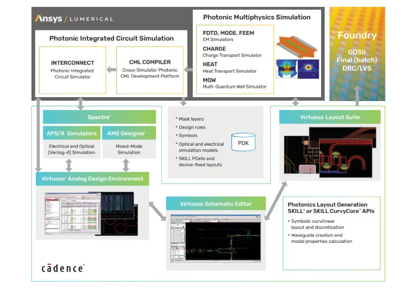
Figure 1: Photonics EDA Workflow Overview (Source: Cadence)
In practice, photonic design closure is driven by the coupling between process assumptions (PDK – where the photonic process design kit defines layer stacks, design rules, and calibrated optical models), model fidelity, and layout-sensitive behaviour. Figure 1 shows why workflows need explicit connections between modelling, simulation, and implementation. Without those links, integration risk tends to surface late, when layout parasitics, thermal drift, or process variation push performance outside the expected envelope.
From Electronic Design to Photonic Design Automation
Electronic design automation evolved around discrete logic, well-defined abstraction layers, and largely deterministic behaviour. Photonic systems violate many of these assumptions.
Optical components are governed by Maxwell’s equations rather than Boolean logic. Behaviour depends on geometry, material properties, wavelength, temperature, and process variation. Photonic circuits are inherently analogue and are frequently coupled with electronics at multiple levels.
Photonics EDA adapts the EDA mindset to this reality. It focuses on physics-aware modelling, continuous simulation, and cross-domain integration rather than purely logical correctness.
Core Elements of a Photonics EDA Stack
Photonic Component Modelling
Photonics EDA begins with accurate component models. Waveguides, modulators, detectors, and resonators are defined in terms of physical parameters rather than abstract logic states. These models must capture dispersion, loss, coupling, and non-linear effects where relevant.
Model fidelity directly affects system predictability. Over-simplified models reduce simulation cost but introduce integration risk later in the programme.
Photonic Design Kits and Process Alignment
Photonic design kits provide the fabrication context. They define layer stacks, design rules, component libraries, and verified process assumptions. Unlike electronic PDKs, photonic PDKs must represent optical behaviour alongside geometric constraints.
Foundry alignment is critical. Minor geometric deviations can shift resonance conditions or coupling efficiency beyond acceptable margins.
Simulation Across Optical and Electrical Domains
Photonics EDA relies on multiple simulation regimes. Frequency-domain solvers analyse steady-state optical behaviour. Time-domain solvers address modulation and transient effects. Circuit-level simulation integrates optical and electrical behaviour within a familiar environment.
The challenge is not running simulations but knowing which approximations are valid at each stage. Excessive fidelity slows iteration. Insufficient fidelity shifts risk downstream into integration and validation.
Layout, Physical Effects, and Manufacturability
Photonic layout is not a cosmetic activity. Geometry defines behaviour. Waveguide bends, crossings, and proximity effects directly influence performance.
Photonics EDA environments must link layout to simulation and design rule checking. Layout-versus-schematic consistency is more complex than in electronics because schematic intent does not uniquely define physical behaviour.
Manufacturability constraints further complicate matters. Yield sensitivity, process corners, and temperature dependence must be considered early, not after tape-out.
Verification Challenges Unique to Photonics
Verification in photonics does not reduce to a pass or fail condition. Optical systems are evaluated against performance envelopes rather than discrete correctness.
Key verification challenges include:
- Wavelength sensitivity across operating bands
- Thermal drift and environmental variation
- Process-induced performance spread
- Interaction between optical and electronic control loops
Photonics EDA supports verification by enabling parametric sweeps, corner analysis, and statistical evaluation. The aim is bounded uncertainty rather than absolute certainty.
Electronic-Photonic Co-Design
Most practical systems are electro-photonic. Control logic, drivers, and signal processing remain electronic, while transmission and modulation increasingly move into the optical domain. This split places tight coupling requirements on timing, control, and physical interfaces across domains.
Photonics EDA must therefore integrate with established electronic workflows, including schematic capture, simulation, and verification. Disconnected toolchains increase integration risk and obscure system-level trade-offs. Co-design enables informed decisions about partitioning, control strategy, and performance margins before physical implementation, when changes are still tractable.
Figure 2: Optical-Electrical Co-Design Loop (Source: researchgate.net )
Optical and electrical domains cannot be designed in isolation. Figure 2 shows how photonic components and electronic control logic interact across both physical and design boundaries. Effective co-design relies on co-simulation, constrained interfaces, and iterative refinement to preserve performance across operating conditions and process variation.
These interactions also change how correctness and confidence must be assessed, particularly when behaviour varies continuously with wavelength and process conditions.
Verification Beyond Pass/Fail
Verification in photonic systems differs fundamentally from digital design. Device behaviour is continuous and highly sensitive to wavelength, temperature, and fabrication variation. As a result, correctness cannot be reduced to discrete pass or fail conditions. Adequate verification instead evaluates performance across operating bands and process corners, making margin, sensitivity, and robustness explicit before fabrication and system integration.
Figure 3: Verification Across Wavelength and Process Corners (Source: researchgate.net )
Figure 3 illustrates this shift in verification focus. Rather than validating a single nominal response, designers examine response envelopes across wavelength and process variation to understand sensitivity and margin. This approach reduces late-stage risk by exposing failure modes before layout finalisation and fabrication handoff.
Scaling from Prototypes to Production
Early photonic designs often succeed as laboratory prototypes but struggle to scale. Photonics EDA addresses this transition by formalising design intent, verification assumptions, and manufacturability constraints.
As designs scale, the cost of late-stage change increases sharply. Photonics EDA reduces this risk by making physical effects visible earlier in the workflow and enabling structured iteration rather than trial-and-error.
Standards, Ecosystems, and Industry Alignment
Photonics EDA does not exist in isolation. It aligns with broader industry initiatives around silicon photonics, heterogeneous integration, and advanced packaging.
Consortium-led efforts and shared frameworks support interoperability, PDK portability, and ecosystem maturity. These reduce duplication of effort and help establish repeatable engineering practice across organisations.
Constraints and Trade-Offs
Photonics EDA introduces its own trade-offs. High-fidelity simulation increases accuracy but slows iteration. Abstraction improves productivity but risks hiding critical physical effects.
Engineering judgement remains central. Tools support decisions but do not replace responsibility. Successful programmes understand where to invest modelling effort and where approximation is acceptable.
Why Photonics EDA Matters at the System Level
Photonics EDA matters because optical integration moves risk upstream. Without disciplined design automation, uncertainty accumulates silently until late-stage validation exposes it.
By structuring modelling, simulation, layout, and verification, photonics EDA enables predictable scaling from concept to deployment. It supports system-level decision-making rather than isolated optimisation.
Continue Exploring
If you would like to explore more work in this area, see the related articles in the Photonics section on the Alpinum website:
https://alpinumconsulting.com/resources/blogs/photonics/
For discussion, collaboration, or technical engagement, contact Alpinum Consulting here:
https://alpinumconsulting.com/contact-us/

Written by : Mike Bartley
Mike started in software testing in 1988 after completing a PhD in Math, moving to semiconductor Design Verification (DV) in 1994, verifying designs (on Silicon and FPGA) going into commercial and safety-related sectors such as mobile phones, automotive, comms, cloud/data servers, and Artificial Intelligence. Mike built and managed state-of-the-art DV teams inside several companies, specialising in CPU verification.
Mike founded and grew a DV services company to 450+ engineers globally, successfully delivering services and solutions to over 50+ clients.
Mike started Alpinum in April 2025 to deliver a range of start-of-the art industry solutions:
Alpinum AI provides tools and automations using Artificial Intelligence to help companies reduce development costs (by up to 90%!) Alpinum Services provides RTL to GDS VLSI services from nearshore and offshore centres in Vietnam, India, Egypt, Eastern Europe, Mexico and Costa Rica. Alpinum Consulting also provides strategic board level consultancy services, helping companies to grow. Alpinum training department provides self-paced, fully online training in System Verilog, UVM Introduction and Advanced, Formal Verification, DV methodologies for SV, UVM, VHDL and OSVVM and CPU/RISC-V. Alpinum Events organises a number of free-to-attend industry events
You can contact Mike (mike@alpinumconsulting.com or +44 7796 307958) or book a meeting with Mike using Calendly (https://calendly.com/mike-alpinumconsulting).
Stay Informed and Stay Ahead
Latest Articles, Guides and News
Explore related insights from Alpinum that dive deeper into design verification challenges, practical solutions, and expert perspectives from across the global engineering landscape.