Introduction: Why photonics now matters to industry
Photonics has moved from a specialist technology into a foundational element of modern industrial systems. This transition has not been driven by novelty or incremental performance gains, but by structural limits in electrical scaling that now dominate system behaviour.
Across computing, manufacturing, communications, and sensing, system architects face the same constraints. Data movement consumes more power than computation. Signal integrity degrades with distance and bandwidth. Thermal margins tighten as integration density increases. These are not implementation details. They are first-order architectural risks.
Photonics addresses these limits directly. Optical transmission decouples bandwidth from resistive loss and electromagnetic interference. Optical sensing enables precision and robustness where electrical methods struggle. Integrated photonics enables these advantages to be manufactured and reproduced with greater consistency, provided integration and packaging are controlled.
Industry forums, including ITF Photonics USA and the Optical Fiber Communication Conference (OFC), increasingly frame photonics not as an alternative technology, but as an infrastructure layer required for system-scale viability. Similar themes appear at European industry forums such as ECOC, where system integration, qualification, and deployment considerations increasingly dominate technical discussion.A separate section at the end lists the conferences and forums referenced in this article, along with dates and locations.
Integrated photonics as an industrial platform
The earliest industrial uses of photonics relied on discrete optical components. While effective, these systems were expensive to assemble, sensitive to alignment, and difficult to qualify at scale. Integration has changed this by shifting optical functionality into repeatable manufacturing flows.
Integrated photonics brings optical waveguides, modulators, detectors, and coupling structures onto a common substrate, often aligned with silicon manufacturing processes. The industrial importance of this shift lies in predictability rather than density. Integrated platforms reduce unit-to-unit variation, offer improved thermal behaviour, and support controlled production flows.
Research and manufacturing roadmaps discussed at forums such as ITF Photonics USA emphasise the importance of mature process platforms, design enablement, and test strategies in moving photonics from laboratory demonstrations into deployable industrial systems. The emphasis has shifted from proving that photonics functions to demonstrating that it can be produced, integrated, and supported with acceptable risk over system lifetimes.
Data movement as the dominant system constraint
In many industrial systems, data movement now consumes more energy than computation at scale and increasingly sets the limits on latency and system growth. Hyperscale computing makes this clear, but the same effect occurs in industrial analytics pipelines, sensor fusion systems, and distributed control architectures. As systems grow, the effort to move data often outweighs that to process it.
Electrical interconnects reach their limits quickly under these conditions. Higher bandwidth forces designers to add equalisation, shielding, and power margin to preserve signal integrity. These measures increase complexity and tighten thermal budgets, yet they do not remove the underlying constraint. The system hits an architectural limit, not an implementation flaw.
Photonics addresses this constraint directly. Optical links sustain high data rates over longer distances while consuming less energy per bit and avoiding electromagnetic interference. This capability allows system architects to reconsider where computation, control, and storage reside. Instead of clustering compute close to data to manage interconnect losses, designers can distribute functions more flexibly without introducing prohibitive latency or power overhead.
These changes affect real design decisions, particularly at the packaging, partitioning, and integration level.
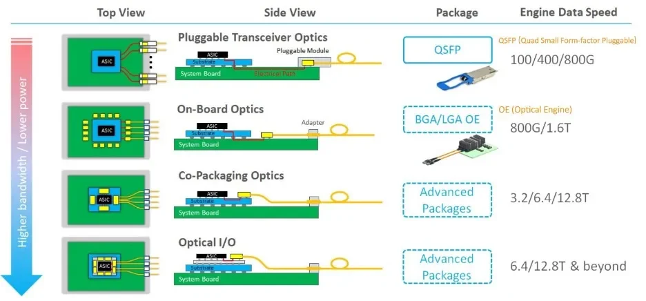
Figure 1: Optical I/O integration models and packaging evolution
Figure 1: Optical I/O integration models and packaging evolution
Conceptual comparison of optical integration approaches, showing the progression from pluggable transceiver optics to on-board optics, co-packaged optics, and direct optical I/O. The diagram highlights how rising data rates and bandwidth density push optical interfaces closer to switching and compute silicon. Source: ASE
Figure 1 shows how optical integration tracks system constraints rather than device innovation. As bandwidth density increases, designers shorten electrical paths and move optical interfaces closer to compute and switching silicon. Each step reflects trade-offs between power efficiency, signal integrity, packaging complexity, and serviceability. These trade-offs now dominate architectural decisions in high-performance and industrial computing systems.
Technical programmes at forums such as the Optical Fiber Communication Conference (OFC) increasingly frame optical interconnects in this way, treating them as architectural enablers that shape system partitioning and scaling, rather than as incremental upgrades to existing links.
Electrical versus optical signal transport at the system boundary
Electrical interconnects move data by transporting charge through conductive paths. As bandwidth and distance increase, resistive loss, capacitive loading, and electromagnetic coupling degrade signal integrity and force additional equalisation, isolation, and power margin. These measures increase complexity and energy consumption while leaving the underlying scaling limit unchanged.
Optical interconnects change the transport mechanism. Data is converted to light at the transmitter, carried optically across the link, and converted back to the electrical domain at the receiver. The optical path itself avoids resistive and electromagnetic penalties, thereby typically improving energy efficiency and enabling higher data rates.
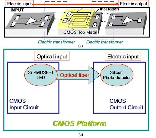
Figure 2: Electrical and optical signal transport in a CMOS platform. Source: stl.tech
Figure 2: Electrical and optical signal transport in a CMOS platform. Source: stl.tech
Comparison of electrical signal transport through CMOS interconnect structures with optical transport using integrated light sources, fibre, and photodetectors.
By separating data transport from electrical signalling, optical links allow designers to move high-bandwidth data across packages and modules without forcing compute and control logic to remain physically adjacent. This capability increasingly determines where and how photonics is introduced as systems scale.
Photonics in industrial sensing and metrology
Industrial sensing has long relied on optical techniques, but tighter integration with control and analytics systems has expanded their role. Optical sensors provide high sensitivity, immunity to electromagnetic interference, and reliable operation in harsh or inaccessible environments where electrical approaches are less effective.
Applications include structural monitoring, precision metrology, spectroscopy-based material analysis, and non-contact inspection. What differentiates modern deployments is not sensing capability alone, but how optical measurements feed directly into digital control and analytics pipelines, rather than terminating at standalone measurement instruments.
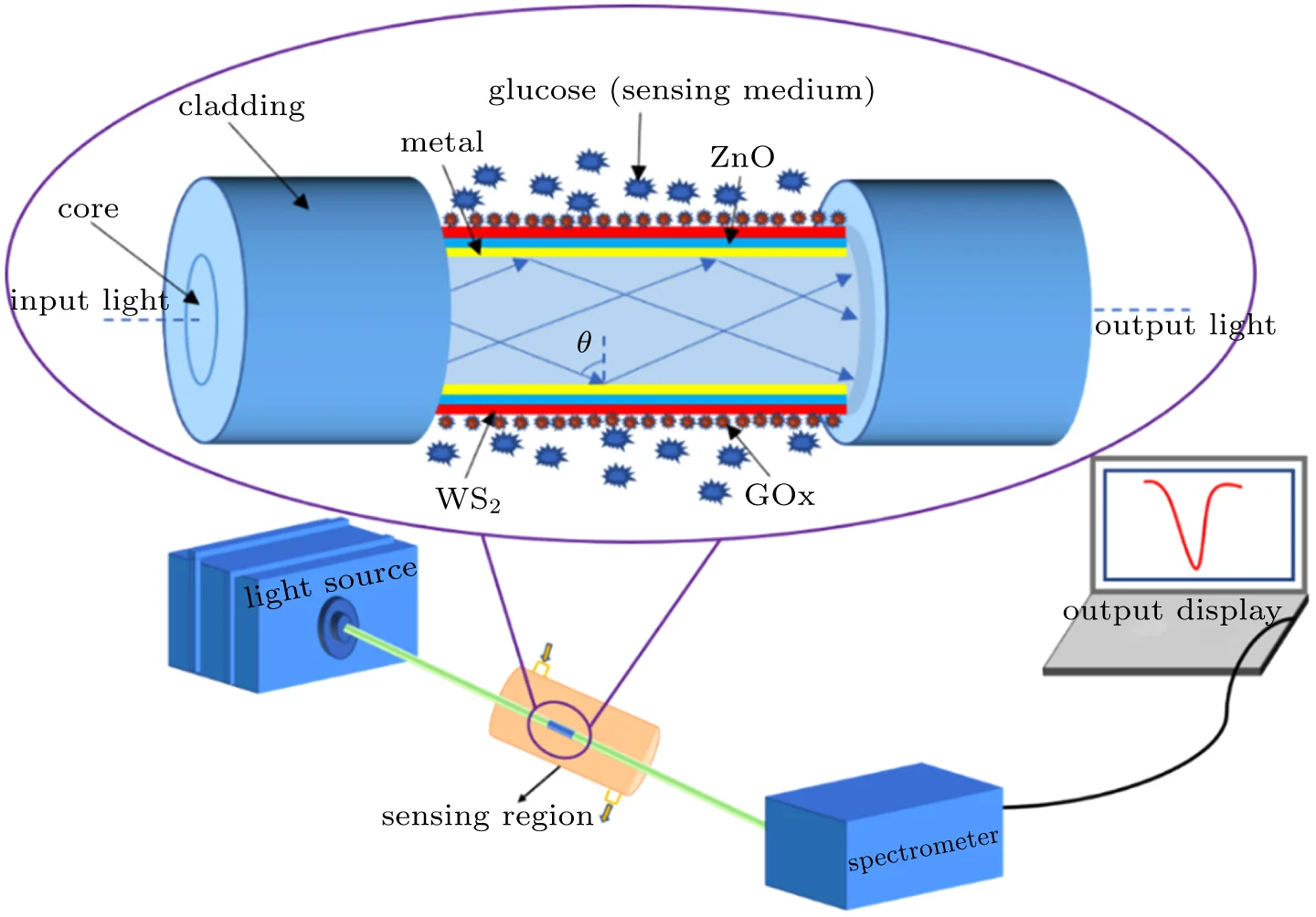
Figure 3: Photonics-based industrial sensing loop. Source: vrogue.co
Figure 3: Photonics-based industrial sensing loop. Source: vrogue.co
Conceptual illustration of an optical sensing loop in which guided light interacts with a functionalised sensing region. Changes in the sensed environment modulate the optical signal, which is detected, digitised, and processed as part of a closed-loop measurement and control system.
Figure 3 shows how this closed-loop structure operates in practice. Light propagates through a waveguide or fibre and interacts with a defined sensing region. Changes in the surrounding environment alter the optical response. Photodetectors convert this response back to the electrical domain, where downstream processing interprets the signal for monitoring or control.
This tight coupling introduces system-level considerations. Optical sensing must be validated alongside electronic control logic and software interpretation layers as part of a single system context. Latency, calibration drift, and failure modes propagate across domains. As a result, photonics increasingly appears in discussions of closed-loop system verification, rather than as an isolated sensing technology.
Communications infrastructure and industrial networking
Industrial communications increasingly resemble large-scale computing systems in both structure and complexity. Deterministic latency, resilience, and long-term reliability are essential in sectors such as energy, transportation, and advanced manufacturing.
Photonics supports these requirements by providing high-capacity backbone links that are less sensitive to noise and environmental interference. Optical fibre and integrated transceivers allow bandwidth scaling without linear increases in power or system complexity.
From a system perspective, photonics enables a more precise separation between the physical transport and protocol layers. This separation reduces coupling between infrastructure upgrades and functional requalification. The result is not just higher bandwidth, but lower programme risk as systems evolve and scale over time.
Manufacturing readiness and ecosystem maturity
The industrial viability of photonics depends on manufacturing maturity as much as on technical capability. Integrated photonics now benefits from process design kits, multi-project wafer access, and standardised test strategies that reflect the evolution of CMOS electronics. These developments move photonics away from bespoke engineering effort and towards repeatable, platform-based integration.
Industry forums, including PIC Summit USA, reflect this shift towards ecosystem readiness. Discussions focus on yield, packaging, co-integration with electronics, and supply-chain stability. These factors determine whether photonics can be deployed at scale as an engineering platform rather than treated as a custom solution for each application.
The growing presence of photonics alongside electronics at mainstream technical forums signals a broader change. Photonics is increasingly treated as part of standard system engineering practice, rather than a specialist or experimental exception.
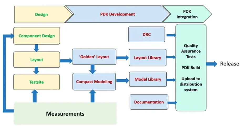
Figure 4: Silicon photonics manufacturing workflow. Source: latitudeds
Figure 4: Silicon photonics manufacturing workflow. Source: latitudeds
High-level view of a silicon photonics design and manufacturing workflow, showing progression from component design and layout through PDK development, modelling, verification, quality assurance, and release.
Figure 4 illustrates how this workflow operates in practice. Component design and layout feed into a controlled “golden” layout, which anchors compact modelling and library development. Measurements close the loop by validating models against fabricated structures, while design-rule checking, documentation, and quality assurance activities ensure that the PDK supports repeatable use. The result is a manufacturable platform rather than a one-off design flow.
This workflow matters because it changes how photonics is introduced into industrial systems. Platform maturity reduces variation, shortens development cycles, and allows photonic components to be qualified alongside electronic subsystems. As a result, photonics increasingly becomes a managed technology layer within broader system engineering and programme qualification flows, rather than a bespoke integration risk carried by individual projects.
System-level trade-offs and risks
Photonics introduces its own constraints. Optical components are often sensitive to temperature and process variation. Co-packaging optics with electronics complicates thermal management and test access. Debugging and observability differ significantly from the electrical domain and require different tooling and assumptions.
These trade-offs require explicit system-level treatment. Successful industrial deployments integrate photonics into architectural decision-making, verification planning, and lifecycle management. Treating photonics as a drop-in replacement for electrical links often shifts risk rather than reducing it.
The organisations that benefit most from photonics are those that align optical design, electronic control, and system verification within a coherent engineering framework with clear ownership and accountability.
Related Industry Conferences and Forums
The following industry conferences and forums reflect where integrated photonics, optical interconnects, and system-level deployment challenges are actively discussed by researchers, system architects, and industrial practitioners. Dates and locations are included for reference.
- ITF Photonics USA
17 March 2026, JW Marriott, Los Angeles, USA
Focuses on integrated photonics manufacturing readiness, optical interconnects, and electronic–photonic co-integration, with emphasis on bridging research capability and scalable industrial deployment. - Optical Fiber Communication Conference (OFC 2026)
15 – 19 March 2026, Los Angeles, California, USA
Covers optical communications, interconnect architectures, and deployment considerations across telecom, data centre, and high-performance computing systems. - SPIE Photonics West
17 – 22 January 2026, San Francisco, California, USA
Broad industry forum addressing photonics manufacturing, integration, sensing, and applied system-level use cases across multiple sectors. - PIC Summit USA
19 January 2026, Sunnyvale, CA 94085, USA
Industry-focused forum covering photonic integrated circuit ecosystems, packaging maturity, co-integration with electronics, and supply-chain readiness. - European Conference on Optical Communication (ECOC 2026)
20 – 24 September 2026, Málaga, Spain, Europe
Focuses on optical communications, network architectures, and system-level deployment of photonics across telecom, data infrastructure, and emerging applications, including AI and quantum technologies
Continue Exploring
If you would like to explore more work in this area, see the related articles in the Photonics section on the Alpinum website:
👉 https://alpinumconsulting.com/resources/blogs/photonics/
For discussion, collaboration, or technical engagement, contact Alpinum Consulting here:
👉 https://alpinumconsulting.com/contact-us/

Written by : Mike Bartley
Mike started in software testing in 1988 after completing a PhD in Math, moving to semiconductor Design Verification (DV) in 1994, verifying designs (on Silicon and FPGA) going into commercial and safety-related sectors such as mobile phones, automotive, comms, cloud/data servers, and Artificial Intelligence. Mike built and managed state-of-the-art DV teams inside several companies, specialising in CPU verification.
Mike founded and grew a DV services company to 450+ engineers globally, successfully delivering services and solutions to over 50+ clients.
Mike started Alpinum in April 2025 to deliver a range of start-of-the art industry solutions:
Alpinum AI provides tools and automations using Artificial Intelligence to help companies reduce development costs (by up to 90%!) Alpinum Services provides RTL to GDS VLSI services from nearshore and offshore centres in Vietnam, India, Egypt, Eastern Europe, Mexico and Costa Rica. Alpinum Consulting also provides strategic board level consultancy services, helping companies to grow. Alpinum training department provides self-paced, fully online training in System Verilog, UVM Introduction and Advanced, Formal Verification, DV methodologies for SV, UVM, VHDL and OSVVM and CPU/RISC-V. Alpinum Events organises a number of free-to-attend industry events
You can contact Mike (mike@alpinumconsulting.com or +44 7796 307958) or book a meeting with Mike using Calendly (https://calendly.com/mike-alpinumconsulting).
Stay Informed and Stay Ahead
Latest Articles, Guides and News
Explore related insights from Alpinum that dive deeper into design verification challenges, practical solutions, and expert perspectives from across the global engineering landscape.