Tessolve AI Strategy
Tessolve’s AI Center of Excellence (CoE) follows a structured strategy to continuously train and improve AI models through iterative learning and validation. The process begins with a rich training dataset, supplemented by recorded user prompts to refine AI responses. The first trained version, Model v1, is developed and undergoes a validation phase using automated test data to assess accuracy and reliability. The validated model generates results, which are analyzed for performance improvements. Insights from this phase guide the infusion of Untrained Model v2 which is new to market but with better efficiencies. The new model undergoes further training and validation to enhance accuracy and adaptability. This even becomes better with recorded prompts and responses from the earlier model. This iterative cycle ensures continuous learning, optimizing AI models to handle real-world design verification and automation challenges. By leveraging automation and AI-driven validation, Tessolve enhances efficiency, minimizes errors, and accelerates verification workflows. This strategy establishes a robust AI framework, making AI-assisted verification more reliable and scalable.
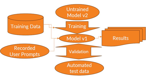
Figure 1: Tessolve CoE AI Strategy
Enhancing Design Verification with AI-Driven Automation
Tessolve is redefining the landscape of semiconductor design verification by integrating artificial intelligence (AI) into its process, according to Bartley et al., (2024). Traditional verification methods often require extensive manual effort, which can be time-consuming and prone to human error. Tessolve’s AI-driven tools automate the generation of test benches, enabling designers to validate their RTL designs quickly and efficiently. By leveraging AI, the verification process is streamlined and made more reliable, reducing the chances of undetected errors in early design stages.
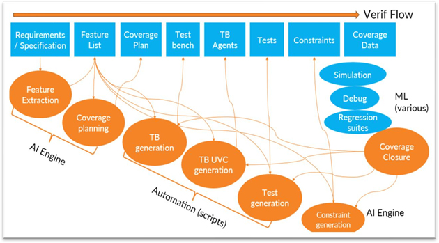
Figure 2: AI Assisted Design Verification Flow
The diagram represents the Design Verification Flow, showcasing how AI, Automation, and Machine Learning (ML) enhance verification efficiency. It begins with Requirements/Specifications, where AI assists in Feature Extraction to generate a Feature List. AI also aids in Coverage Planning, ensuring a well-structured Coverage Plan. Automation scripts handle Testbench (TB) and UVC generation, reducing manual effort and improving test quality. AI further automates Test Generation and Constraint Generation, ensuring comprehensive verification. The generated tests feed into Simulation, Debug, and Regression Suites, where ML optimizes the results. ML-driven analysis enables faster Coverage Closure, reducing verification cycles. AI engines ensure efficiency, accuracy, and adaptability across the verification process. The integration of AI and automation minimizes human intervention, accelerating time-to-market. This structured flow streamlines verification, ensuring robust chip validation.
Independent Verification for Robust Design Validation
Ensuring independent verification is a crucial step in design validation, as it eliminates biases and potential blind spots from designers, as highlighted by Bartley et al., (2024). Tessolve’s AI tools help generate test benches from RTL specifications in Verilog, System Verilog (SV), or Universal Verification Methodology (UVM), ensuring a structured and systematic approach to verification. Designers can integrate key verification components like assertions, functional coverage, and scoreboard functions, which verification engineers can choose to reuse or modify as needed. This approach fosters a collaborative verification process while distinguishing between design and verification roles.

Figure 3: Tool for AI generated Testbenches and Integrated Simulation with Open-Source Tool
Coverage Optimization with Machine Learning
One of the key challenges in design verification is achieving high coverage with minimal effort, as mentioned by Bartley et al., (2024). Tessolve employs machine learning (ML) techniques such as Gradient Descent and Genetic Algorithms to optimize verification goals. AI ensures that RTL designs achieve better functional coverage by analyzing test results and iteratively improving test scenarios. This intelligent approach reduces verification cycles and enhances overall test effectiveness, allowing engineers to focus on more complex validation tasks.
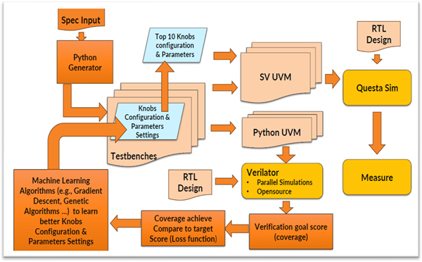
Figure 4: Coverage Improvement using ML
Seamless Integration and Accelerated Debugging
Tessolve’s AI-driven tools seamlessly integrate with existing tool chains, enabling smooth compilation and simulation workflows, as emphasized by Bartley et al., (2024). The built- in error feedback system allows real-time debugging, helping designers identify and fix issues faster. By automating smoke tests, designers can independently verify their designs without waiting for dedicated DV teams, reducing verification bottlenecks and accelerating the development cycle. Combining automation and intelligent debugging leads to significant time and resource savings for semiconductor companies.
The Future of AI in Semiconductor Verification
According to Bartley et al., (2024), Tessolve develops its AI strategy based on adaptability and continuous improvement principles. By incorporating replaceable AI models, centralized AI services, and customizable solutions, Tessolve ensures that its tools remain at the forefront of innovation. The company’s commitment to leveraging open- source technologies provides the industry with cost-effective and flexible verification solutions. Tessolve is revolutionizing how semiconductor companies ensure their RTL designs’ accuracy and reliability with its cutting-edge design verification approach as AI continues to evolve.
Note: To learn more about Tessolve’s AI-driven verification solutions, visit our website: www.tessolve.com.
References
Bartley, M., Soni, M., C Tessolve. (2024). AI Strategy for DV Flow & TB AI Tool. https://www.tessolve.com/